N-pin structure semiconductor luminous diode

A technology for light-emitting diodes and light-emitting regions, which is applied to semiconductor devices, electrical components, circuits, etc., and can solve the problems of not obtaining the current spreading effect, reducing the brightness of the device by the current spreading layer, and failing to obtain current spreading.

Inactive Publication Date: 2005-03-02
BEIJING UNIV OF TECH
View PDF0 Cites 8 Cited by
  • Summary
  • Abstract
  • Description
  • Claims
  • Application Information

AI Technical Summary

Problems solved by technology

Obviously, using a thin metal layer as the current spreading layer can neither get good current spreading, but also introduces absorption loss, usually about 50% loss, which is why this thin metal layer is called a semi-transparent layer.
The current spreading layer prepared by this method greatly reduces the brightness of the device, and does not get a good current spreading effect

Method used


Image

  • N-pin structure semiconductor luminous diode
  • N-pin structure semiconductor luminous diode
  • N-pin structure semiconductor luminous diode

Examples


Embodiment 1

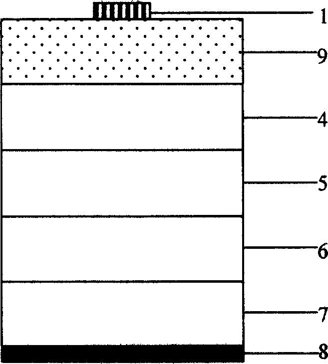
[0034] Such as Figure 5 As shown, the realization method of the n-pin structure red light-emitting diode is as follows:

[0035] 1. Using common metal-organic chemical vapor deposition (MOCVD) method in n + -GaAs substrate 7 epitaxially grows n-AlInP lower confinement layer 6, AlGaInP heterojunction light-emitting region 5, p-AlInP upper confinement layer 4, p + -GaAs / n + - GaAs tunnel junction 3 and n-GaP current spreading layer 2;

[0036] 2. Use a Karl Suss lithography machine to lithography the mask pattern.

[0037] 3. By conventional evaporation method, ohmic contact electrode 1 Au / Ge / Ni / Au is evaporated on the front side;

[0038] 4. Using the conventional stripping method, there is only metal left at the ohmic contact electrode 1;

[0039] 5. The sample is thinned to 100 μm by conventional mechanochemical corrosion method;

[0040] 6. Evaporate the upper and lower ohmic contact electrodes 8 Au / Ge / Ni / Au on the substrate 7 according to the conventional process;

...

Embodiment 2

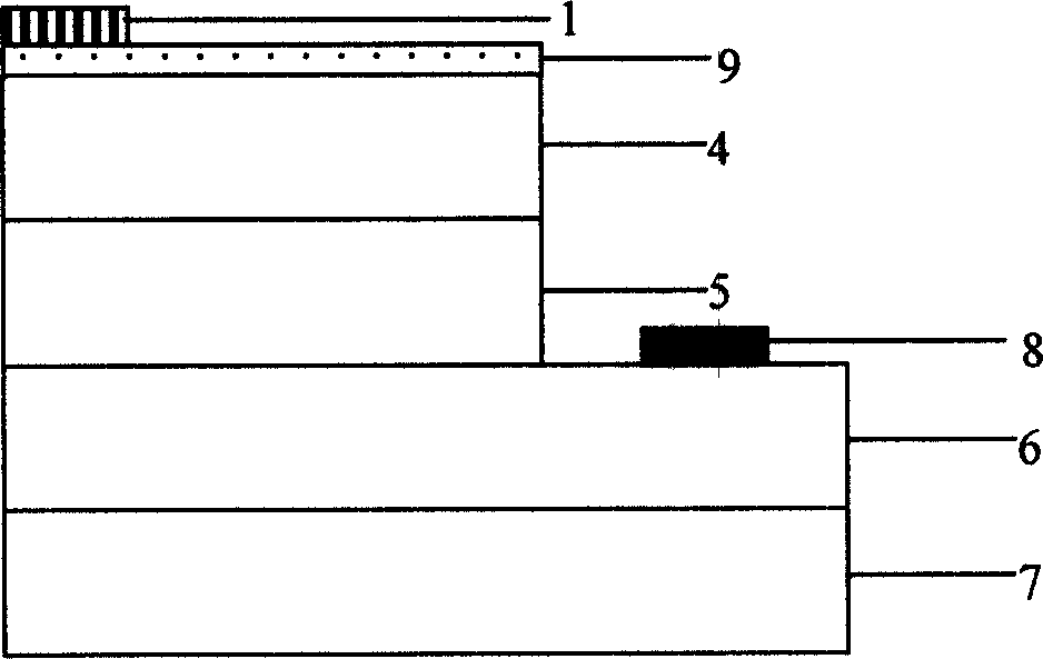
[0044] Such as Figure 7 As shown, the realization method of n-pin structure blue light-emitting diode is as follows

[0045] 1. Epitaxially grow the n-GaN lower confinement layer 6, the InGaN / GaN quantum well light-emitting region 5, and the p-GaN upper confinement layer 4 on the sapphire substrate 7 sequentially by ordinary metal-organic chemical vapor deposition (MOCVD). + -InGaN / n + - InGaN tunnel junction 3, and n-GaN current spreading layer 2;

[0046] 2. Use a conventional Karl Suss lithography machine to photoetch mask patterns for dry etching;

[0047] 3. Use Oxford (Oxford) ICP-100 to etch the sample out of the mesa structure to 6 places of the n-GaN lower confinement layer, the etching gas is chlorine and argon, the etching time is 10 minutes, and the etching depth is 600 nanometers;

[0048] 4. Obtain the shapes of the upper and lower ohmic contact electrodes 1 and 8 by photolithography according to the conventional process;

[0049] 5. The upper and lower ohmi...


PUM


Abstract

The n-pin structure semiconductor LED consists of longitudinal stacked upper ohm contact electrode, P type upper limit layer, red or blue lighting region, n type lower limit layer, substrate and lower ohm contact electrode. The characteristic is longitudinal arranged n-current spreading layer and tunnel junction between upper ohm contact electrode and p type upper limit layer. By the invention, thickness of current spreading layer is reduced, once epitaxial growth is realized, component prodn. process of GaN LED is simplified.

Description

technical field [0001] An n-pin structure semiconductor light-emitting diode (LED) belongs to the technical field of semiconductor optoelectronics. Background technique [0002] Light-emitting diodes are widely used in information indication, information display and information transmission due to their remarkable characteristics such as long life, high efficiency, small size, and environmental protection, especially in white light lighting, showing huge market potential and Application prospects. At present, red and blue light emitting diodes prepared by AlGaInP / GaAs material system and GaN-based material system respectively have become the most efficient red and blue light emitting diodes. [0003] According to the working principle of light-emitting diodes, its basic layer structure is mainly a p-i-n heterostructure, that is, a p-type upper confinement layer, an i-type light-emitting region and an n-type lower confinement layer. Usually, the thickness of the p-type upper...

Claims


Application Information

Patent Timeline
Patent Type & Authority Applications(China)
IPC IPC(8): H01L33/00H01L33/14H01L33/38
Inventor 郭霞沈光地邓军邹德恕徐遵图李建军刘莹杜金玉
Owner BEIJING UNIV OF TECH
Why Eureka
Try Eureka