Process for the manufacture of Er doped / Er, Yb codoping aluminium oxide optical wave guide amplifier

An optical waveguide amplifier and aluminum oxide technology, applied in lasers, laser components, optics, etc., can solve the problems of low cost performance and single function

Inactive Publication Date: 2005-06-01
DALIAN UNIV OF TECH
View PDF0 Cites 2 Cited by
  • Summary
  • Abstract
  • Description
  • Claims
  • Application Information

AI Technical Summary

Problems solved by technology

However, most products have single fun

Method used


Image

  • Process for the manufacture of Er doped / Er, Yb codoping aluminium oxide optical wave guide amplifier
  • Process for the manufacture of Er doped / Er, Yb codoping aluminium oxide optical wave guide amplifier
  • Process for the manufacture of Er doped / Er, Yb codoping aluminium oxide optical wave guide amplifier

Examples


Embodiment

[0020] Step 1. Thermal oxidation of silicon substrate

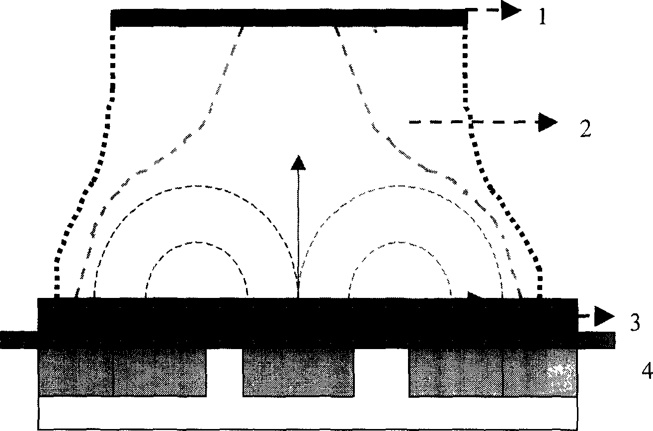
[0021] In order to enable light waves to propagate in the thin film sample, the refractive index of the substrate needs to be lower than that of the thin film sample, usually by depositing a layer of SiO on a single crystal silicon wafer. 2 . In the experiment, thermal oxidation method was used to oxidize SiO with a thickness of about 600nm. 2 . The specific experimental process is as follows:

[0022] 1. Cleaning:

[0023] A. Clean with acetone and ethanol first, and then clean with ultrasonic wave for 5 minutes.

[0024] B. HF acid diluent cleaning.

[0025] C. Boil concentrated sulfuric acid for 3 minutes.

[0026] 2. Dry oxygen:

[0027] Put the monocrystalline silicon into the dry oxygen furnace and feed it with oxygen to heat it to make it react. The chemical equation of the reaction is Dry oxygen time 5 minutes.

[0028] 3. Wet oxygen:

[0029] After dry oxygen, there is a thin layer of SiO on the su...


PUM


Abstract

The present invention belongs to the field of active optical amplifier device in optical communication technology, and is especially one kind of Er doped or Er and Yb doped aluminan optical waveguide amplifier and its preparation process. The present invention features that the optical waveguide amplifier is prepared through MF plasma magnetically controlled sputtering to prepare Er doped or Er and Yb doped alumina film; annealing of the prepared film; and mask etching process including five steps of depositing SiO2 layer on the film, painting photoresist, ultraviolet irradiating to decomposing SiO2 under mask to form etching pattern, etching the substrate in plasman and eliminating photoresist. The present invention may be used for the compensating amplification of optical signal in optical communication to serve as repeater.

Description

technical field [0001] The invention belongs to the technical field of active optical amplifier devices in optical communication technology, and specifically relates to a method for preparing erbium / erbium and ytterbium co-doped alumina optical waveguide amplifiers by means of intermediate frequency plasma magnetron sputtering and mask etching . Background technique [0002] In optical fiber communication systems, there is loss when optical signals are transmitted in optical fibers. Therefore, in practical applications, a "repeater" must be installed every tens of kilometers to amplify the attenuated optical signal and continue to transmit it along the optical fiber line. The rare earth Er 3+ inner 4f electrons 4 I 13 / 2 - 4 I 15 / 2 The energy level transition of the silica fiber has a characteristic wavelength of 1.54 μm, which is just in the lowest loss region of the silica fiber. It is an ideal transmission band for optical fiber communication, and the outer electrons...

Claims


Application Information

Patent Timeline
IPC IPC(8): G02F1/39H01S3/00
Inventor 李成仁宋琦宋昌烈李建勇李淑凤
Owner DALIAN UNIV OF TECH
Why Eureka
Try Eureka