Method for fabricating tube core of light emitting diode in gallium nitride substrate through technique of reverse filling welding

A light-emitting diode, gallium nitride-based technology, applied in electrical components, circuits, semiconductor devices, etc., can solve the problems of small heat dissipation area, affecting the working performance and life of the die, etc.

Inactive Publication Date: 2005-06-15
INST OF SEMICONDUCTORS - CHINESE ACAD OF SCI
View PDF0 Cites 8 Cited by
  • Summary
  • Abstract
  • Description
  • Claims
  • Application Information

AI Technical Summary

Problems solved by technology

This preparation method needs to etch the N-type mesa, and the heat dissi...

Method used


Image

  • Method for fabricating tube core of light emitting diode in gallium nitride substrate through technique of reverse filling welding
  • Method for fabricating tube core of light emitting diode in gallium nitride substrate through technique of reverse filling welding
  • Method for fabricating tube core of light emitting diode in gallium nitride substrate through technique of reverse filling welding

Examples


Embodiment Construction

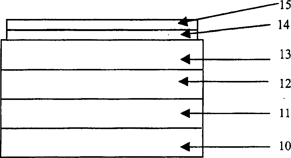
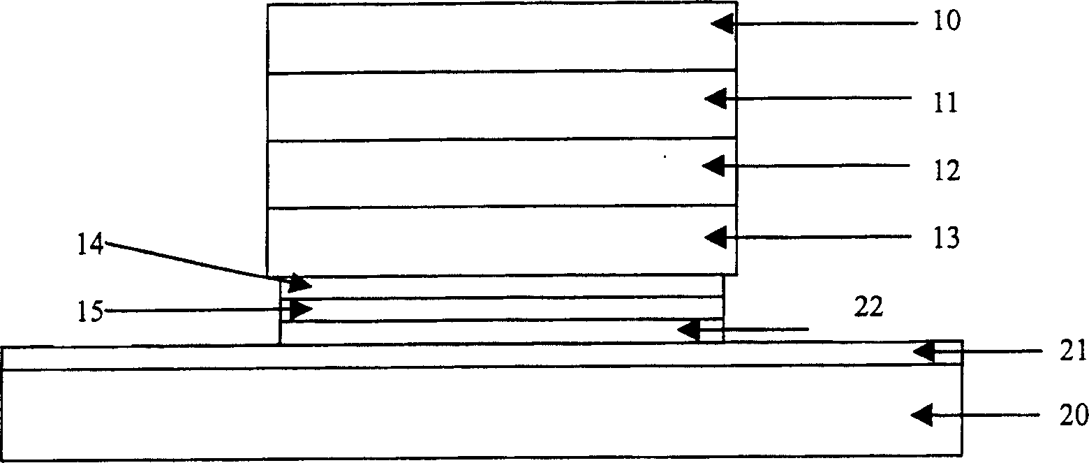
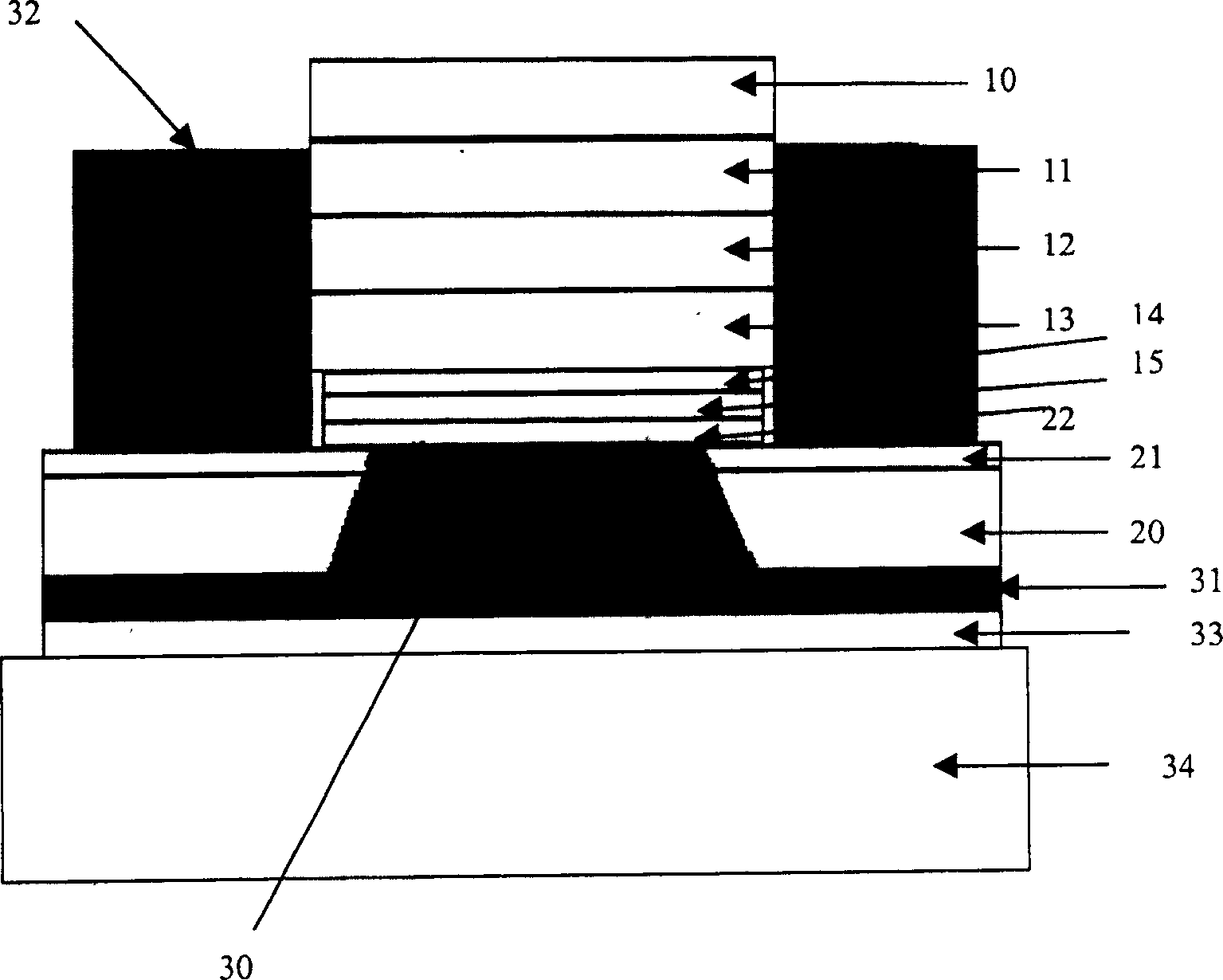
[0026] The invention discloses a method for preparing gallium nitride-based light-emitting diode tube cores by flip-chip welding technology, which is characterized in that, compared with the traditional technology, holes are opened on the tube core support body for flip-chip soldering, and nitrogen The P-type electrode of the gallium nitride-based light-emitting diode is drawn from the back of the die support, and the side surface of the N-type layer of the epitaxial structure of the gallium nitride-based light-emitting diode is used as the contact area of ​​the N-type ohmic contact electrode of the die, and the die The back of the support body is welded to the heat sink. This method of manufacturing the die can save the etching process steps of the N-type contact area of ​​the die in the traditional manufacturing process technology, increase the light output area, and be used in flip-chip welding Holes are opened on the die support body, and the P-type electrode is drawn out f...


PUM

PropertyMeasurementUnit
Thicknessaaaaaaaaaa
Thicknessaaaaaaaaaa

Abstract

The method includes following steps: (1) N-type gallium nitride layer, luminescence active region and P type gallium nitride layer is developed on sapphire etc. insulated substrate; (2) P-type ohmic contact electrode is prepared on P-type gallium nitride layer in tube core; (3) sapphire insulated substrate is thinned to between 70 micros to 150 micros; (4) brazing metal layer in size correspondent to size of P type ohmic contact electrode in tube core is vaporized on a supporter, where silicon dioxide or silicon nitride etc. dielectric isolation layer is deposited on; (5) hole is prepared on P-type ohmic contact electrode in tube core, vaporizing or plating metal layer on back face of the supported with hole being made, and P-type electrode in tube core is led out; (6) a metal layer is deposited on side at back face of tube core reverse welded through photo etching and evaporation method; (7) welding P-type ohmic contact electrode in supporter of single tube core to heat sink.

Description

technical field [0001] The invention belongs to the technical field of semiconductors, in particular to a method for manufacturing gallium nitride-based light-emitting diode tube cores by flip-chip welding technology. Background technique [0002] III-V gallium nitride (GaN)-based compound semiconductors and their quantum well structure light-emitting diodes (LEDs) have the advantages of high reliability, high efficiency, long life, full solidification, and low power consumption. There is a huge application market in the field of lamp information indication and general light display and indication, especially the combination of GaN-based purple or blue light-emitting diodes and phosphors can be made into white light diodes, which has a potential application market in the lighting field and is expected to replace Today's incandescent and fluorescent lamps have become green lighting sources in the 21st century. In order to meet the lighting requirements in the future, GaN lig...

Claims


Application Information

Patent Timeline
IPC IPC(8): H01L33/00
Inventor 杨辉张书明王良臣
Owner INST OF SEMICONDUCTORS - CHINESE ACAD OF SCI
Why Eureka
Try Eureka