Piezoelectric element, ink jet head, angular velocity sensor, and ink jet recording apparatus
A technology of piezoelectric elements and piezoelectric layers, applied in the manufacture/assembly of piezoelectric devices/electrostrictive devices, electrical components, piezoelectric/electrostrictive devices, etc., can solve problems such as cracking and achieve reliable Improved performance and good piezoelectric properties
- Summary
- Abstract
- Description
- Claims
- Application Information
AI Technical Summary
Problems solved by technology
Method used
Image

Examples
Embodiment 1
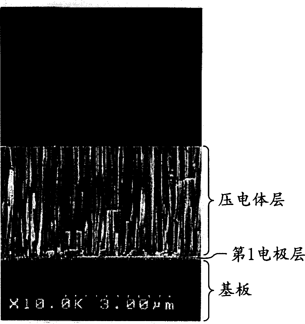
[0143] In Example 1, the material, film thickness, manufacturing method, etc. of each film are the same as those described in the above-mentioned Embodiment 1. Immediately after the completion of the production, no cracks or film peeling were observed in the respective films of the piezoelectric element of Example 1.
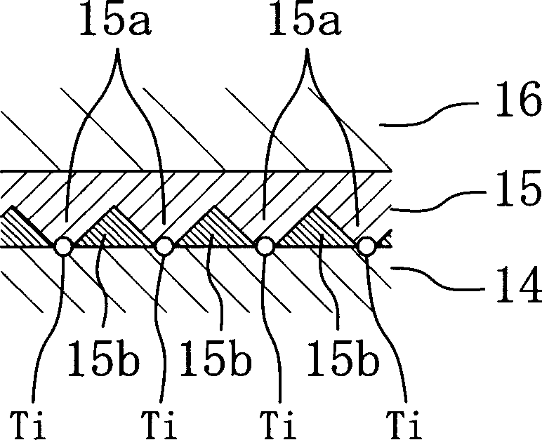
[0144] The crystal orientation and film composition of the piezoelectric layer before forming the second electrode layer were studied. That is, according to the analysis by the X-ray diffraction method, the piezoelectric layer showed a (100) plane-oriented triangular perovskite type crystal structure, and the (100) plane orientation degree was α=97%. In addition, composition analysis with an X-ray microanalyzer revealed that the composition of the piezoelectric layer was the same as that of the target, the ratio of Zr / Ti was 55 / 45, and the ratio of Mg / Nb was 33 / 67.
[0145] Further, the crystal structure of the piezoelectric layer was analyzed with a scanning e...
Embodiment 2
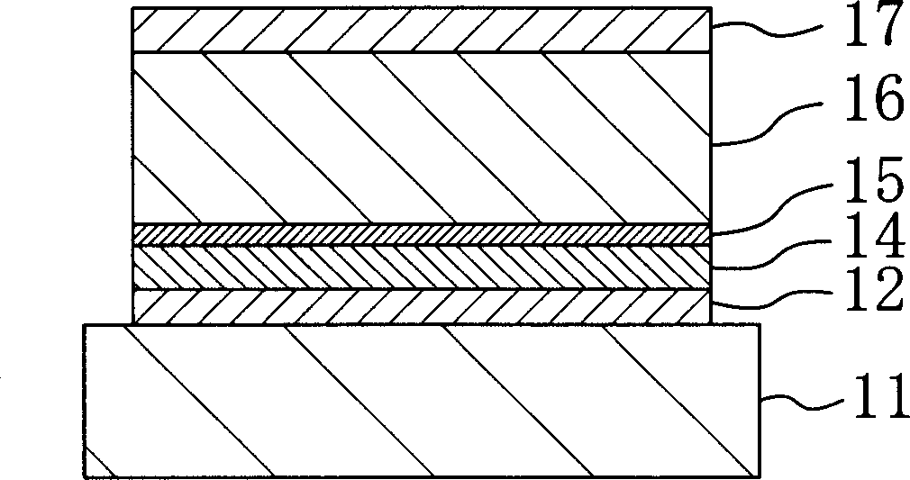
[0158]In Example 2, the substrate is 0.25 mm thick and is 4 inches of stainless steel (SUS304), the adhesion layer uses a tantalum (Ta) film with a film thickness of 0.01 micron; the first electrode layer uses a film thickness of 0.25 micron, containing A Pt film of 8 mol% titanium oxide; the orientation control layer uses a PLT film with a film thickness of 0.03 microns, containing 17 mol% of lanthanum, and an excess of 6 mol% of the lead content compared to the stoichiometric composition (3 mol% of magnesium is added); 0.8PZT(Zr / Ti=40 / 60)-0.2Pb(Mg 1 / 3 Nb 2 / 3 )O 3 film; a Pt film with a film thickness of 0.1 μm was used for the second electrode layer.
[0159] Using a Ta target, in an argon gas of 1 Pa, the substrate was heated to 500° C. and a high-frequency power of 100 W was applied for 1 minute to obtain the above-mentioned adhesion layer.
[0160] Using a multi-target sputtering device, using a titanium target and a Pt target, while heating the substrate to 400 ° C,...
Embodiment 3
[0174] In Example 3, the substrate is barium borosilicate glass (100 mm square size) with a thickness of 0.5 mm, and the adhesive layer uses a nickel (Ni) film with a film thickness of 0.005 micron; the first electrode layer uses a film thickness of 0.15 micron, An iridium (Ir) film containing 18 mol% of titanium; the orientation control layer uses a PLT film (adding 1 mol% of manganese) with a film thickness of 0.02 microns, containing 8 mol% of lanthanum and an excess of 16 mol% in lead content compared to the stoichiometric composition; The electrode layer uses 0.9PZT (Zr / Ti=40 / 60)-0.1Pb(Ni 1 / 3 Nb 2 / 3 )O 3 For the second electrode layer, a Pt film with a film thickness of 0.01 μm was used.
[0175] Using a Ni target, in an argon gas of 1 Pa, the substrate was heated to 300° C. and a high-frequency power of 200 W was applied for 1 minute to obtain the above-mentioned adhesion layer.
[0176] Using a multi-target sputtering device, in an argon gas of 1 Pa, the substrate wa...
PUM
| Property | Measurement | Unit |
|---|---|---|
| Piezoelectric constant | aaaaa | aaaaa |
| Film thickness | aaaaa | aaaaa |
| Piezoelectric constant | aaaaa | aaaaa |
Abstract
Description
Claims
Application Information
 - R&D Engineer
- R&D Manager
- IP Professional
- Industry Leading Data Capabilities
- Powerful AI technology
- Patent DNA Extraction
Browse by: Latest US Patents, China's latest patents, Technical Efficacy Thesaurus, Application Domain, Technology Topic.
© 2024 PatSnap. All rights reserved.Legal|Privacy policy|Modern Slavery Act Transparency Statement|Sitemap