Structure and manufacture of resistance(R) - capacitance(C) - diode(D) network thin-film IC with transverse venting diode

A technology of integrated circuits and diodes, which is applied in the field of microelectronic integrated circuit semiconductor devices, and can solve problems such as difficulty in manufacturing and incompatibility with the manufacturing process of semiconductor devices

Inactive Publication Date: 2006-02-08
HEILONGJIANG BADA UNIVERSAL SEMICON
View PDF0 Cites 6 Cited by
  • Summary
  • Abstract
  • Description
  • Claims
  • Application Information

AI Technical Summary

Problems solved by technology

Compound materials such as TaN and CrSi are used to make resistors, because they are dif

Method used


Image

  • Structure and manufacture of resistance(R) - capacitance(C) - diode(D) network thin-film IC with transverse venting diode
  • Structure and manufacture of resistance(R) - capacitance(C) - diode(D) network thin-film IC with transverse venting diode
  • Structure and manufacture of resistance(R) - capacitance(C) - diode(D) network thin-film IC with transverse venting diode

Examples


Embodiment Construction

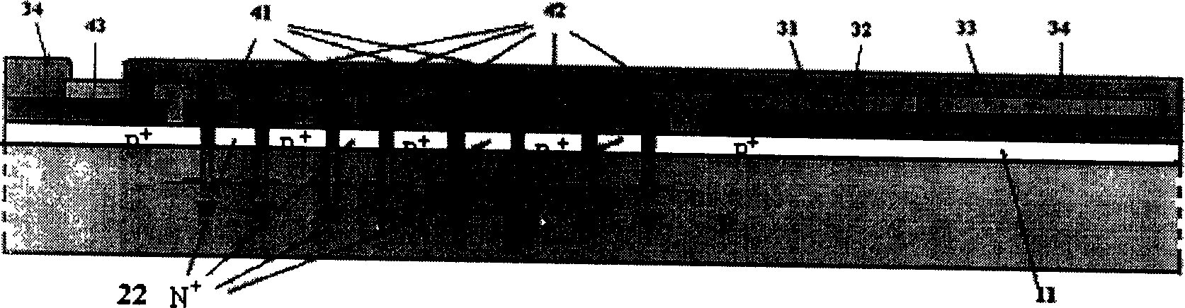
[0024] The resistance-capacitance-diode network thin film integrated circuit of the present invention has good anti-static discharge damage function and anti-electromagnetic radiation function, and the anti-static ability exceeds 5000V, which can completely protect the electrostatic discharge generated by the human body.

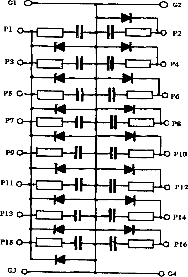
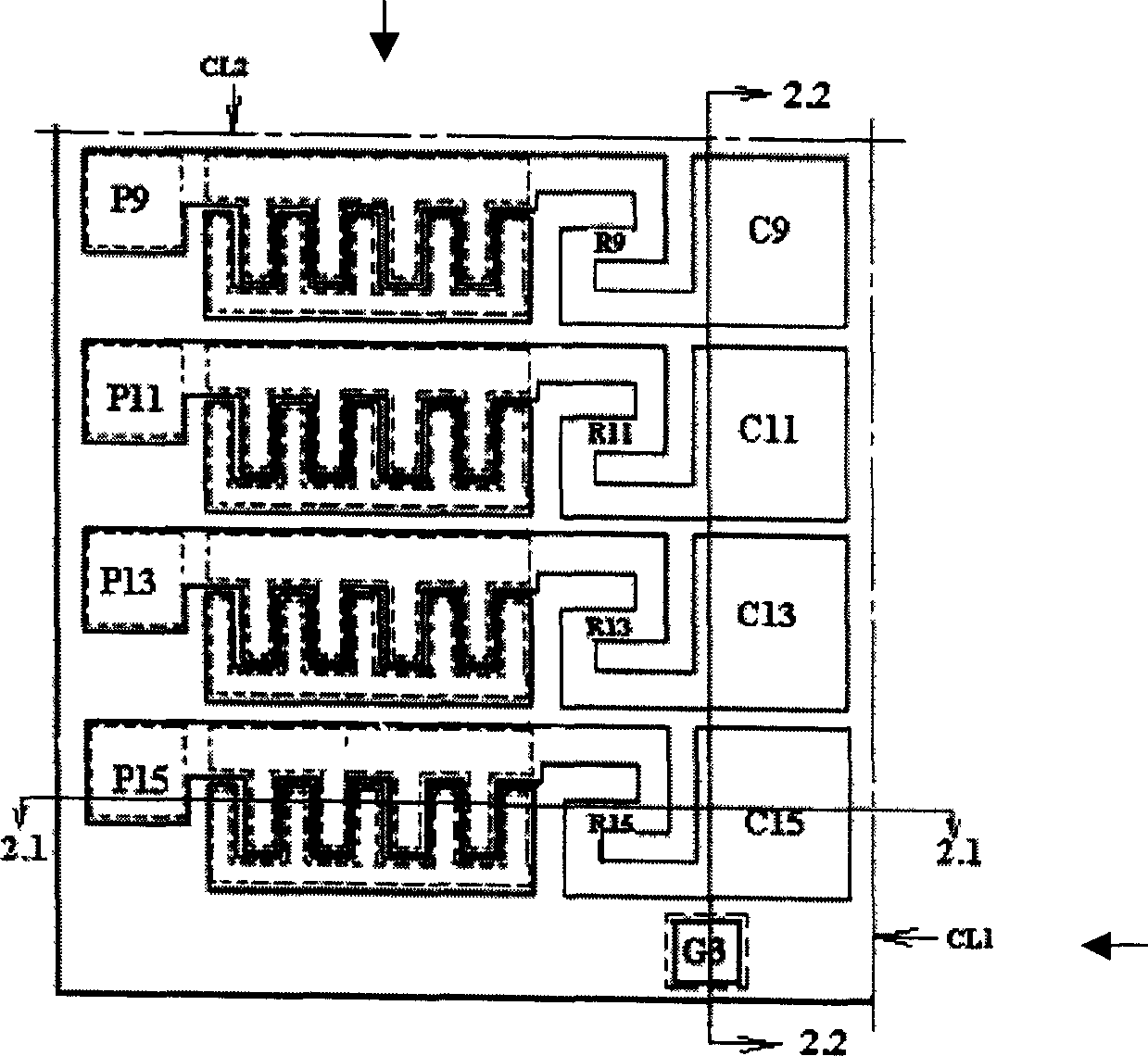
[0025] figure 1 The shown RCD network circuit can be processed into a semiconductor RCD network thin film integrated circuit chip according to the semiconductor manufacturing method provided by the present invention. The RCD network can be used as a filter to reduce electromagnetic and radio frequency interference, eliminate negative pulse voltage spikes and reduce high data transmission noise, etc. figure 1 , figure 2 Provide the circuit diagram and structure and component distribution diagram of the embodiment of the present invention;

[0026] Among them, there are 16 resistors and 16 capacitors Ci (i=1, 2...16) with the same value, and 16 diodes Di (i...


PUM


Abstract

The invention discloses a resistance(R)-electric capacity(C) net thin-film integrated circuit structure that comprises crosswise diodes and the preparing method, adopting common silicon pellet (P) to prepare network thin-film integrated circuit of high conductive layer and over voltage protection. P+ area (11) formed with boron diffusion works as the public ground conductive layer, base of the crosswise diode (D) and bottom electrode of the capacitor (C). N+ area (22) formed with phosphor diffusion works as emitter area of the crosswise diode. The W area between P+ and N+ area is the lead area of the diode with reverse bias voltage. Prepare SiO2 and Si3N4 insulating dielectric medium (31) by means of chemical vapor deposition (CVD) on the surface of silicon pellet. The aluminum layer is taken as metallic layer, after photo etching, forming internal connection leads of circuit, pressure point are aluminum layer (43) and ground (G) press welding point. Deposition phosphor doping SiO2 (34) forms chip inactivation layer, preparing chip after photo-etching press welding point (43) and grounding point (G).

Description

Technical field: [0001] The invention belongs to the technical field of microelectronic integrated circuit semiconductor devices, and relates to passive element resistance (R), capacitor (C) and diode (D) networks, which are manufactured into "RCD" network thin film integrated circuits by using semiconductor thin film technology. technical background: [0002] In various electronic information products, the number of passive components accounts for more than 90% of all components, especially in today's portable and wireless electronic products such as mobile phones, digital cameras, computers and other digital products, passive components The proportion is larger. They occupy a large area of ​​the printed circuit board of the whole machine and have many solder joints, which increase the production cost of the whole machine and reduce the reliability. Driven by the increasing market demand for high frequency, high speed, multi-function, high performance, high reliability, lo...

Claims


Application Information

Patent Timeline
IPC IPC(8): H01L27/02H01L21/82
Inventor 刘振茂陶盛孙芳魁丁峰李开国赵晖金妍
Owner HEILONGJIANG BADA UNIVERSAL SEMICON
Why Eureka
Try Eureka