Organic / macromolecule top emission light-emitting device and its application

A light-emitting device and top-emission technology, which is applied in the direction of organic semiconductor devices, semiconductor/solid-state device manufacturing, and luminescent materials, can solve the problems of complex manufacturing process and easy damage to the light-emitting layer, and achieve simple manufacturing process, good environmental stability, The effect of high quantum efficiency

Inactive Publication Date: 2006-02-08
GUANG ZHOU NEW VISION OPTO ELECTRONICS TECH
View PDF3 Cites 30 Cited by
  • Summary
  • Abstract
  • Description
  • Claims
  • Application Information

AI Technical Summary

Problems solved by technology

In terms of sputtering, there is also a technology that does not use ITO, but sputters zinc-doped indium oxide (IDIXO). This method also has the problem of easily damaging the light-emitting layer (Asuka Yamamori, Sachiko Hayashi, Toshiki Koyama, and Yoshio Taniguchi, Appl. Phys. Lett. 78, 3343 (2001); Takashi Hirano, US6774561)
In addition, there is also the use of plasma technology to form an insulating nitride layer on the surface of the cathode, which significantly improves the performance of the device, but this manufacturing process is relatively complicated and has strict requirements on the plasma time of the device substrate (Samil KHO, Sunyoung SOHN and Donggeun JUNG, Jpn. J. Appl. Phys. 42, 552 (2003))

Method used


Image

  • Organic / macromolecule top emission light-emitting device and its application
  • Organic / macromolecule top emission light-emitting device and its application
  • Organic / macromolecule top emission light-emitting device and its application

Examples


Embodiment 1

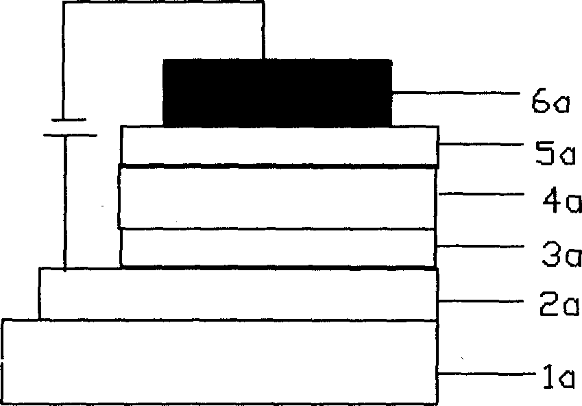
[0062] ITO conductive glass, sheet resistance ~ 20Ω / □, or ordinary glass without ITO, pre-cut into 15mm×15mm square pieces. Sequentially use acetone, special detergent for micron semiconductors, deionized water, and isopropanol to ultrasonically clean, nitrogen purged, then placed in a constant temperature oven for standby, and further processed in an oxygen plasma cleaner before use.

[0063] After weighing the fluorescent conjugated polymer in a clean bottle, transfer it to a nitrogen-protected film-forming glove box (VAC company), dissolve it in toluene, and filter it with a 0.45 micron filter membrane. The optimal thickness of the polymer light-emitting layer is 70-90 nanometers. The film thickness was measured with a TENCOR ALFA-STEP-500 surface profiler. PFNBr-BTDZ05, PFN-BTDZ05, PF-N + R 3 , PF-NR 2 Dissolve them in methanol respectively, and prepare three solutions with concentrations of 0.02%, 0.1%, and 0.2%. Use the uniformly glue machine to rotate the pre -stea...

Embodiment 2

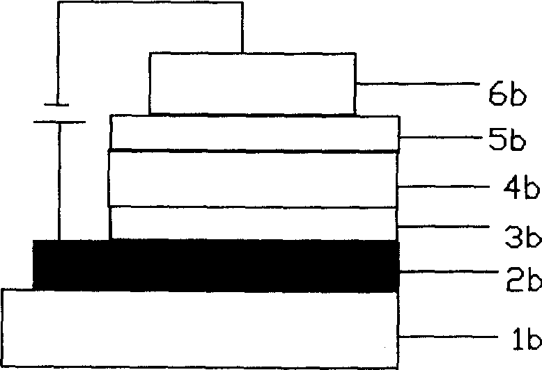
[0082] Repeat Example 1, but the polymer light-emitting layer is replaced by green light-emitting phenyl-substituted poly-p-phenylene vinylene (P-PPV), and the electron injection layer uses PFNBr-BTDZ05 or neutral precursor PFN-BTDZ05 respectively. The experimental results are summarized in Table 6 and Table 7, respectively.

[0083] Table 6 is based on the green light material P-PPV, using aluminum as the cathode, using gold as the transparent anode, and using

[0084] Emissive

layers

Thickness

()

Cathode

A node

Voltage

(V)

Current

(mA)

Luminance

(cd / m2)

QE

(%)

P-PPV

P-PPV

P-PPV

50

100

200

Al

Al

Al

Au

Au

Au

24.2

26.5

30

12.6

29.1

3.61

155

2738

128

0.16

1.2

0.45

[0085]The top-emitting light-emitting device structure in Table 6 is ITO / Al / PFNBr-BTDZ05 / P-PPV...

Embodiment 3

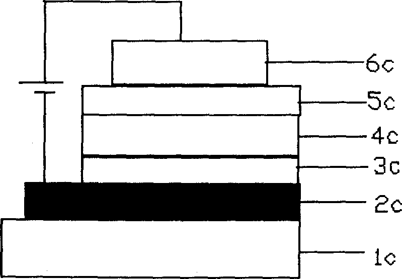
[0093] Repeat Example 2. The polymer light-emitting layer was replaced by polyfluorene (PFO) that emits blue light, and poly[9,9-dioctylfluorene-9,9-bis(N,N-dimethylaminopropyl)fluorene] A three-component copolymer with a narrow band gap (narrow band gap monomer benzothiadiazole) (PFN-BTDZ05) was used as the electron injection layer. The experimental results are summarized in Table 8. Figure 9(a) is a graph of voltage-current-luminescence luminance of a top-emitting light-emitting device using PFN-BTDZ05 as the electron injection layer, blue-emitting polyfluorene (PFO), aluminum as the cathode, and gold as the transparent anode. Fig. 9(b) is the electroluminescence spectrum of the top emission light-emitting device.

[0094] Table 8 is based on the blue light material PFO, using aluminum as the cathode, using gold as the transparent anode, and using PFN-BTDZ05

[0095] Emissive

layers

Thickness

()

Cathode

A node

Voltag...


PUM

PropertyMeasurementUnit
thicknessaaaaaaaaaa

Abstract

This invention discloses an organic macromolecule top light emitting device, which comprises a glass substrate, a negative pole, a light-emitting layer, a positive pole, characterized in that: an electron layer is located between the positive pole and light-emitting layer adopting conjugated polymer of polar monomer with polar gene or ionic gene. The invention discloses the application of the top light-emitting device in high-resolution full color top emitting monitor, characterized in: using a high work function metal negative pole on the substrate and a conjugated polymer of strong polarity component with polarity gene or ionic gene, actualizing effective electron injection, via desposit the electroluminescence emits in the transparent positive pole, with stable efficiency.

Description

technical field [0001] The invention relates to a novel top-emitting light-emitting device, in particular to an organic / polymer top-emitting light-emitting device and its application. Background technique [0002] In 1990, the research team of the University of Cambridge first made the first polymer light-emitting device with a conjugated structure PPV polymer material as the light-emitting layer. Because light-emitting polymer devices have outstanding advantages such as low material cost, easy large-area molding, low driving voltage, low energy consumption, and luminescent wavelength can be tuned through material structure, it is considered possible to be applied in large-area flat-panel TVs. [0003] With the progress of global organic / polymer light-emitting devices in the process of flat-panel display applications, the development of high-efficiency top-emitting light-emitting devices has become one of the urgent research topics. Because compared...

Claims


Application Information

Patent Timeline
Patent Type & Authority Applications(China)
IPC IPC(8): H05B33/00H05B33/14H05B33/22H01L33/00H01L51/00
CPCH05B33/22C09K11/06H01L2251/5315C09K2211/1483H01L51/5092C09K2211/1416C08G61/02C09K2211/1491H10K50/171H10K2102/3026
Inventor 曹镛侯林涛黄飞彭俊彪
Owner GUANG ZHOU NEW VISION OPTO ELECTRONICS TECH
Why Eureka
Try Eureka