Method for making GaN-based LED with back hole structure

A light-emitting diode, gallium nitride-based technology, applied in the field of semiconductors, can solve problems such as hindering high-power light-emitting diodes and large thermal resistance

Active Publication Date: 2006-04-05
YANGZHOU ZHONGKE SEMICON LIGHTING
View PDF0 Cites 6 Cited by
  • Summary
  • Abstract
  • Description
  • Claims
  • Application Information

AI Technical Summary

Problems solved by technology

Although this method solves the problem of heat dissipation to a certain extent, its thermal resistance is still very large, forming a bottleneck that hinders the realization of high-power light-emitting diodes used in general lighting in the future.

Method used


Image

  • Method for making GaN-based LED with back hole structure
  • Method for making GaN-based LED with back hole structure
  • Method for making GaN-based LED with back hole structure

Examples


Embodiment

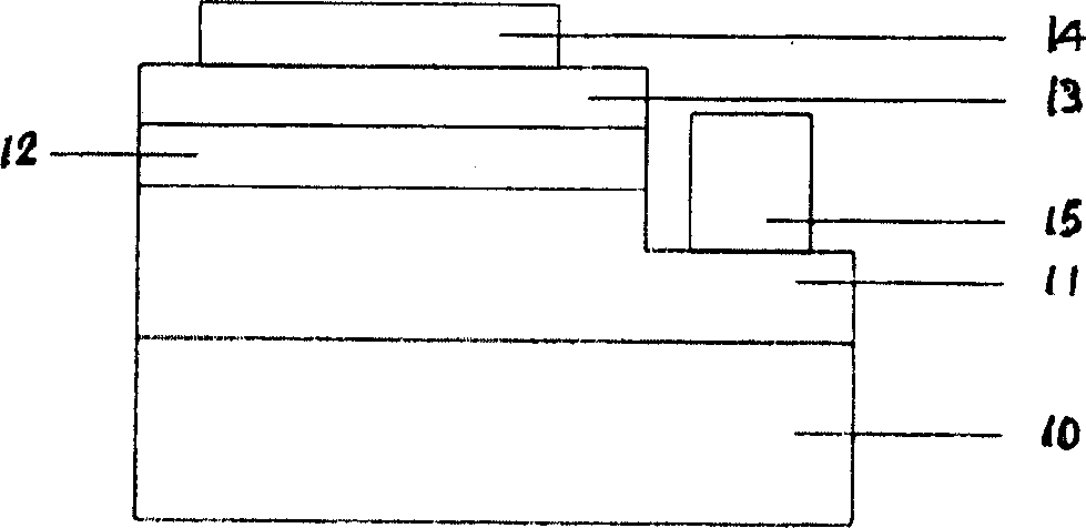
[0041] first as figure 1 As shown, this is a cross-sectional view of the die structure of a GaN-based light-emitting diode. The manufacturing process is to epitaxially grow a GaN N-type contact layer 11 on a sapphire substrate 10 using MOCVD method, a light-emitting active region 12 and a P-type GaN contact layer 13; the shape of the die is designed to be a square, with a size of 1mm×1mm, and then an N-type mesa (N-type contact layer 11) is etched according to the designed die pattern and dry-etched by an ICP system. Ni / Au / Ag / Ni / Au (50 Å / 50 Å / 1500 Å / 200 Å / 1200 Å) was prepared by electron beam evaporation (or sputtering) on ​​the P-type GaN contact layer 13, and annealed at 500 degrees Celsius For 5 minutes, an ohmic contact electrode 14 of P-type GaN with low ohmic contact and high reflectivity is formed. Ti / Al / Ni / Au (150 Å / 2200 Å / 400 Å / 500 Å) was prepared on the N-type GaN layer 11 by electron beam evaporation (or sputtering), and annealed at 900 degrees Celsius for 30 secon...


PUM


Abstract

Disclosed a manufacturing method of gallium nitride light-emitting diode in the back hole structure comprises: N type gallium nitride layer which sequentially extends on the insulating substrate of blue stone, multiple quantum trap luminous active region and a P type gallium nitride layer; processing photo-etching on the N type gallium nitride layer to preparing the P type ohm contact electrode and N type ohm contact electrode; the scribing divides the tube core of epitaxial slice into single tube core; forming a silicon dioxide insulating dividing layer on the two surfaces of silicon slice while preparing the metal electrode on the right face and light etching the back-hole pattern on the back surface; forming the back holes; utilizing the thick paste to light etch and electric plate the protruding point pattern on the right face of silicon slice; preparing a layer of alloy with lower fusible point on the back of silicon to form the tube base; connecting the back of tube base and the tube housing via heat sink; welding the tube core and the right surface of tube base via the metal protruding point, educing the N electrode of light-emitting diode from the metal electrode made on the right surface of silicon slice and educing the P electrode of light-emitting diode from the heat sink back surface of tube housing.

Description

technical field [0001] The invention belongs to the technical field of semiconductors, and relates to a method for manufacturing a GaN-based light-emitting diode with a back hole structure. Background technique [0002] With the breakthrough of the third-generation semiconductor material gallium nitride and the advent of blue, green, and white light-emitting diodes, following the microelectronics revolution triggered by semiconductor technology, a new industrial revolution-the lighting revolution, whose symbol is the semiconductor Lamps will gradually replace incandescent and fluorescent lamps. Semiconductor lamps use light-emitting diodes (LEDs) as new light sources. Under the same brightness, the power consumption is only 1 / 10 of that of ordinary incandescent lamps, but the life span can be extended by 100 times. Because semiconductor lighting (also known as solid-state lighting) has the advantages of energy saving, long life, maintenance-free, and environmental protectio...

Claims


Application Information

Patent Timeline
Patent Type & Authority Applications(China)
IPC IPC(8): H01L33/00H01L33/62H01L33/64
CPCH01L2933/0075H01L2924/01079H01L24/17H01L2924/12041Y10S977/759H01L2224/16H01L33/64H01L2924/01019H01L2924/01029H01L2924/01078H01L33/0079H01L2924/10253H01L33/62H01L2224/05573H01L2224/13025H01L2224/05568H01L2224/05624H01L2224/05644H01L2224/05647H01L2224/05655H01L2224/05666H01L2224/05671H01L2924/00014H01L2224/0554H01L33/0093H01L2924/00H01L2224/05599H01L2224/0555H01L2224/0556
Inventor 马龙王良臣王立彬郭金霞伊晓燕
Owner YANGZHOU ZHONGKE SEMICON LIGHTING
Why Eureka
Try Eureka