Polishing composition and method for polishing a conductive material

A technique for polishing compositions and conductive material layers, applied in polishing compositions containing abrasives, chemical instruments and methods, circuits, etc., capable of solving problems such as yield loss and time increase

Inactive Publication Date: 2006-10-04
APPLIED MATERIALS INC
View PDF13 Cites 27 Cited by
  • Summary
  • Abstract
  • Description
  • Claims
  • Application Information

AI Technical Summary

Problems solved by technology

Some defects can be minimized by reducing these variables, but at the cost of increased time and lost yield

Method used


Image

  • Polishing composition and method for polishing a conductive material
  • Polishing composition and method for polishing a conductive material
  • Polishing composition and method for polishing a conductive material

Examples


Embodiment

[0173] To further describe the embodiments of the present invention, the following non-limiting examples are provided. However, these examples are not complete and are not intended to limit the scope of the present invention.

[0174] Polishing composition example / baseline

[0175] Baseline Example

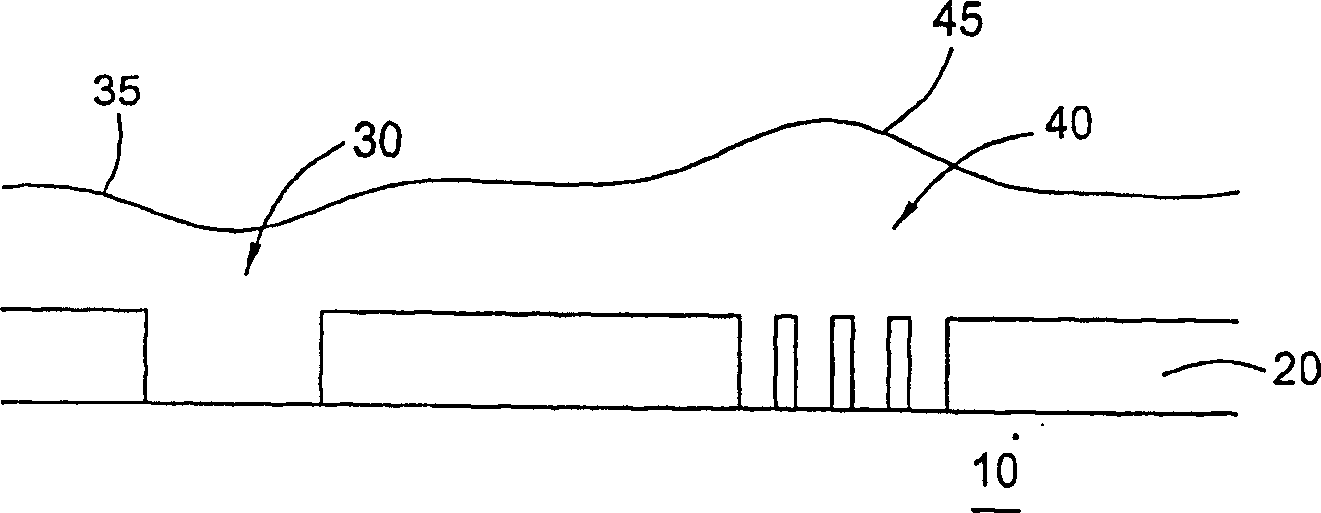
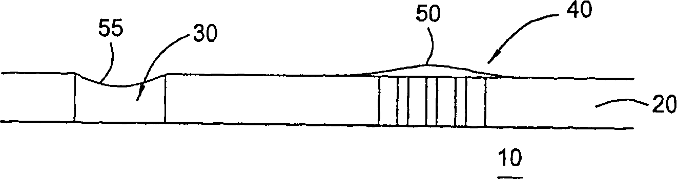
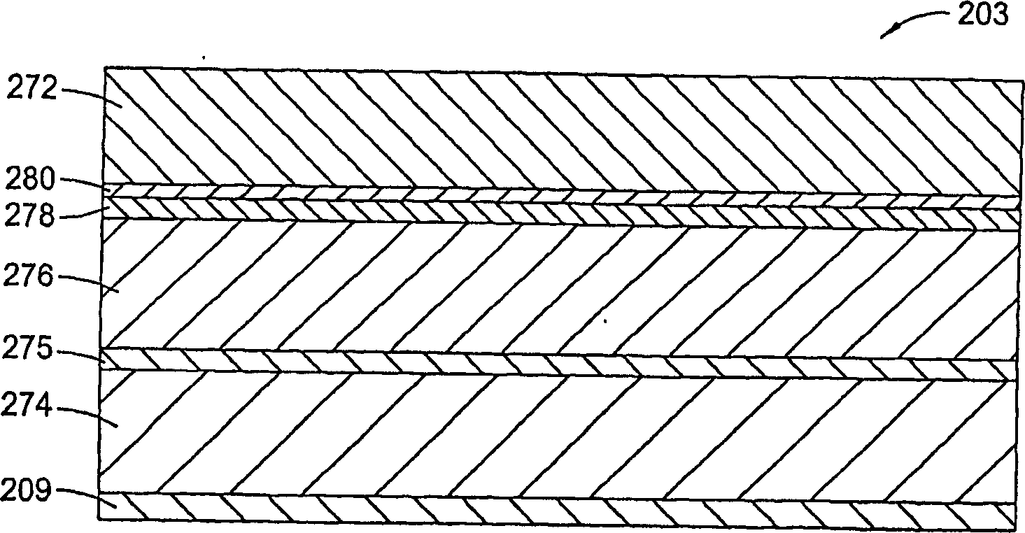
[0176] In one embodiment of the present invention, the substrate 208 is placed in a polishing composition that includes an acid-based electrolyte system, one or more chelating agents, one or more corrosion inhibitors, a One or more pH adjusters, one or more additives, solvents or a combination thereof. An anode bias voltage of about 2.9 volts with respect to the electrode 209 is applied to the surface of the substrate by using the power supply 200. A pressure of 0.2 psi is applied to the substrate through the polishing head 202 to push it toward the conductive pad 203. The substrate 208 and the conductive pad 203 move relative to each other. The combination of the above elements of th...

example 1

[0187] In Reflection purchased from Applied Materials, Inc. of Santa Clara, California  In the improved unit on the system, the following polishing composition is used to polish and planarize the copper-clad substrate.

[0188] About 6% phosphoric acid by volume;

[0189] About 2% by volume of ethylenediamine;

[0190] About 2% by weight of ammonium citrate;

[0191] About 0.3% by weight of benzotriazole;

[0192] Between about 2% and about 6% by volume of potassium hydroxide to provide a pH of about 5; and

[0193] Deionized water.

example 2

[0195] In Reflection purchased from Applied Materials, Inc. of Santa Clara, California  In the improved unit on the system, the following polishing composition is used to polish and planarize the copper-clad substrate.

[0196] About 6% phosphoric acid by volume;

[0197] About 2% by volume of ethylenediamine;

[0198] About 2% by weight of ammonium citrate;

[0199] About 0.3% by weight of benzotriazole;

[0200] Potassium hydroxide between about 2% and about 6% by volume to provide a pH of about 5;

[0201] About 0.45% hydrogen peroxide by volume; and

[0202] Deionized water.


PUM

PropertyMeasurementUnit
sizeaaaaaaaaaa
sizeaaaaaaaaaa
diameteraaaaaaaaaa

Abstract

A method of processing a substrate having a conductive material layer disposed thereon is provided which includes positioning the substrate in a process apparatus and supplying a first polishing composition between to the substrate. The polishing composition comprises phosphoric acid, at least one chelating agent, a corrosion inhibitor, a salt, an oxidizer, abrasive particulates, at least one pH adjusting agent to provide a pH from about 4 to about 7 and a solvent. The method further includes forming a passivation layer on the conductive material layer, removing the passivation layer to expose a portion of the conductive material layer, applying a first bias to the substrate, and removing at least about 50% of the conductive material layer. The method further includes separating the substrate from the first polishing composition, exposing the substrate to a second polishing composition and a second bias, and continuing to remove the conductive material layer.

Description

Technical field [0001] The invention relates to a composition and method for removing conductive material from a substrate. Background technique [0002] Reliable manufacturing of sub-half micron and smaller line widths is one of the key technologies for the next generation of semiconductor devices in Very Large Scale Integration (VLSI) and Ultra Large Scale Integration (ULSI). However, with the advancement of circuit technology limits, the shrinking interconnect size in VLSI and ULSI technologies has placed additional requirements on processing capabilities. The reliable formation of interconnections is important to the success of VLSI and ULSI, as well as to continuous efforts to improve the quality and circuit density of individual substrates and dies. [0003] The technique of sequentially depositing and removing materials on the surface of the substrate is used to form features therein, thereby forming multi-level interconnects. As the material layers are sequentially deposi...

Claims


Application Information

Patent Timeline
Patent Type & Authority Applications(China)
IPC IPC(8): C09G1/02C09K3/14H01L21/3213H01L21/321B23H5/08
CPCC09G1/02H01L21/304H01L21/30625H01L21/687
Inventor 丰·Q·刘陈梁韵斯坦·D·蔡阿莲恩·度布斯特森·S·诺胡永崎王艳保罗·D·布特尔菲尔德
Owner APPLIED MATERIALS INC
Why Eureka
Try Eureka