
Method for manufacturing compound semiconductor substrate

A manufacturing method and semiconductor technology, applied in semiconductor/solid-state device manufacturing, semiconductor devices, electrical components, etc., can solve the problems of transistor diode rectification characteristic electronic device performance degradation, reliability degradation, etc., to achieve excellent performance and reliability, temperature Small rise and excellent heat dissipation effect

Inactive Publication Date: 2006-11-29
SUMITOMO CHEM CO LTD
View PDF0 Cites 3 Cited by
  • Summary
  • Abstract
  • Description
  • Claims
  • Application Information

AI Technical Summary

Problems solved by technology

It is known that if these electronic devices operate at a high current density, the temperature of the electronic device will rise, and the performance of the electronic device such as the current amplification factor of the transistor and the rectification characteristic of the diode will decrease and the reliability will decrease.

Method used


Image

  • Method for manufacturing compound semiconductor substrate
  • Method for manufacturing compound semiconductor substrate
  • Method for manufacturing compound semiconductor substrate

Examples


Embodiment 1

[0052] [Manufacturing of compound semiconductor substrates]

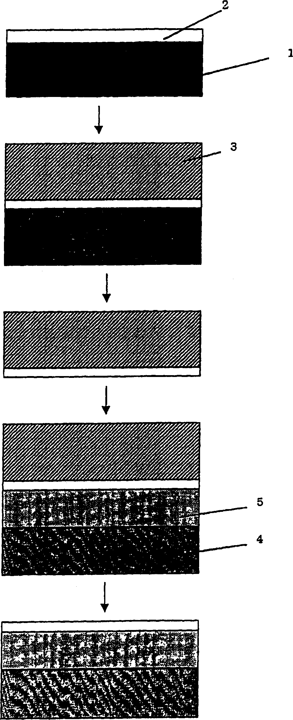
[0053] figure 1 Indicates the process of manufacturing compound semiconductors.

[0054] On a commercially available single crystal semi-insulating GaAs substrate 1 with a diameter of 100mm and a thickness of 630μm, trimethylgallium, triethylgallium, trimethylaluminum, trimethyl Indium, as the starting raw material containing V group elements, uses arsine (arsine) and phosphine trihydride, and as the raw material of the dopant for controlling conductivity, disilane (n-type control), trichlorobromide Methane (p-type control), organometallic vapor phase pyrolysis method used with hydrogen carrier gas, to grow the compound semiconductor functional layer 2 of the heterojunction bipolar transistor, and to manufacture the compound semiconductor substrate. The layer structure of the compound semiconductor functional layer 2 is as follows from the side of the substrate 1:

[0055] Non-doped GaAs layer 50nm

[0056] Non-...

Embodiment 2

[0075] [Manufacturing of compound semiconductor substrates]

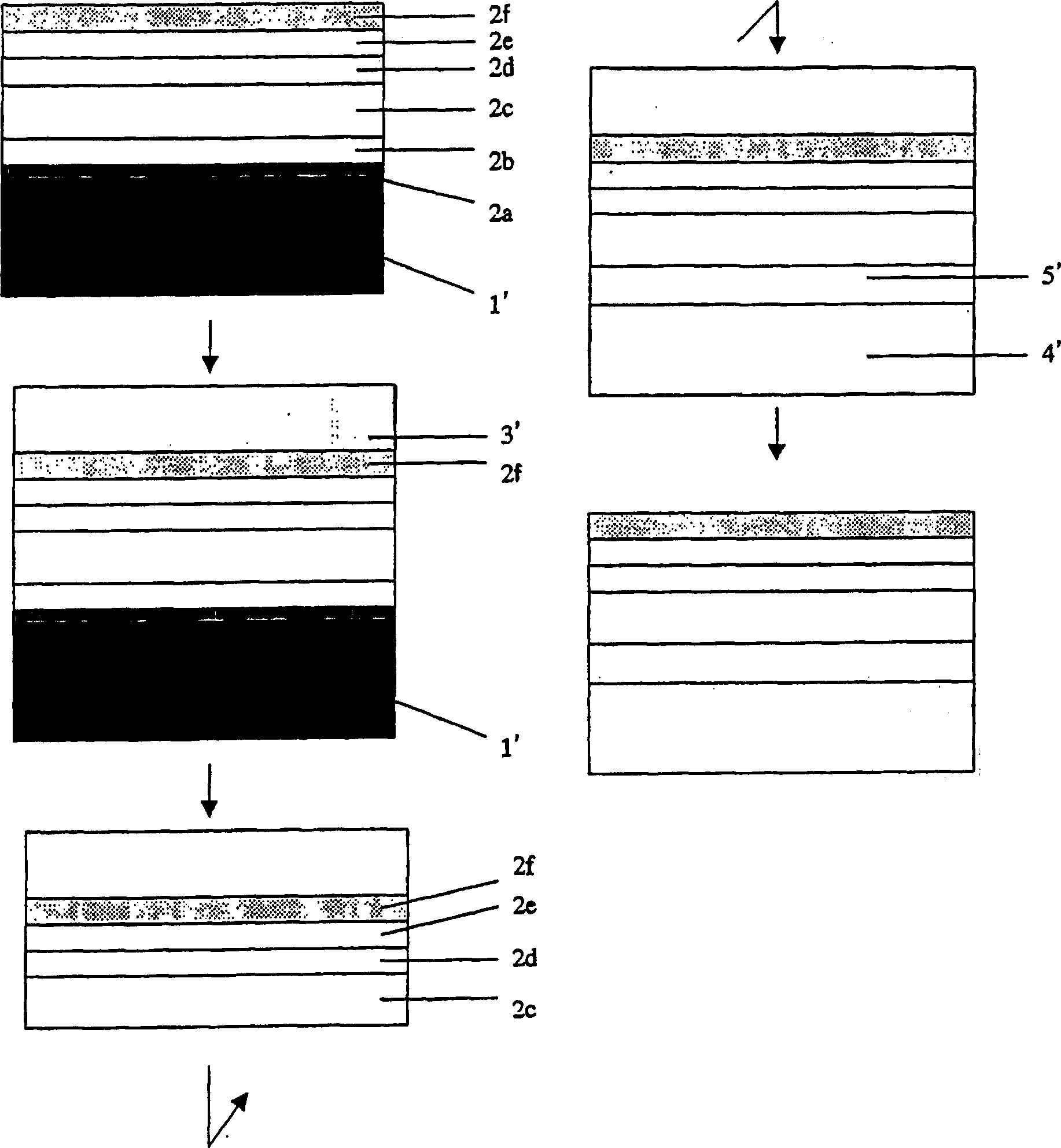
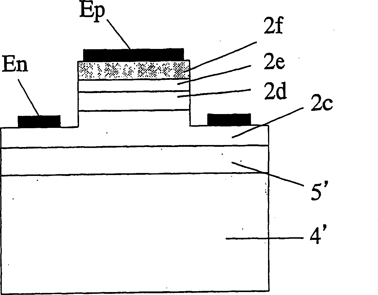
[0076] On a commercially available single-crystal insulating sapphire substrate 1' with a diameter of 50nm and a thickness of 500μm, trimethylgallium and trimethylaluminum were used as starting materials containing group III elements, and trimethylgallium and trimethylaluminum were used as starting materials containing group V elements. As a raw material, ammonia is used as a raw material for dopants to control conductivity, and silane (n-type control), cyclopentadiene-magnesium (p-type control), organometallic vapor phase thermal decomposition used with hydrogen carrier gas In this method, the compound semiconductor functional layer 2' of a pn junction diode is grown to produce a compound semiconductor substrate. The structure of the compound semiconductor functional layer 2' (refer to figure 2 ) from the substrate 1' side as:

[0077] Non-doped GaN buffer layer 2a 20nm

[0078] Non-doped GaN layer 2b 500nm

...


PUM


Abstract

Disclosed is a method for manufacturing a compound semiconductor substrate which comprises the following steps (a)-(e): (a) a compound semiconductor functional layer (2) is epitaxially grown on a substrate (1); (b) a supporting substrate (3) is bonded to the compound semiconductor functional layer (2); (c) the substrate (1) and a part of the compound semiconductor functional layer (2) which is in contact with the substrate (1) are removed by polishing; (d) a multilayer substrate is obtained by bonding a highly heat-conductive substrate (such as a substrate composed of a Si or sapphire substrate (4) and a diamond thin film (5)) having a thermal conductivity higher than that of the substrate (1) to the surface of the compound semiconductor functional layer (2) which is exposed in the step (c); and (e) the supporting substrate (3) is separated from the multilayer substrate.

Description

technical field [0001] The present invention relates to a method for manufacturing a compound semiconductor substrate. Background technique [0002] Compound semiconductor substrates are used in the manufacture of electronic devices such as field effect transistors and heterojunction bipolar transistors. It is known that when these electronic devices operate at a high current density, the temperature of the electronic device rises, and the performance and reliability of the electronic device, such as the current amplification factor of the transistor and the rectification characteristic of the diode, decrease. In order to reduce the temperature rise of electronic devices, a method of manufacturing a compound semiconductor substrate excellent in heat dissipation is being studied. Contents of the invention [0003] An object of the present invention is to provide a method for simply manufacturing a compound semiconductor substrate excellent in heat dissipation. [0004] Th...

Claims


Application Information

Patent Timeline
Patent Type & Authority Applications(China)
IPC IPC(8): H01L21/331H01L21/329H01L21/02H01L21/20H01L21/335H01L29/20H01L29/737
CPCH01L29/66462H01L29/2003H01L21/2007H01L21/185H01L21/02H01L21/18H01L21/20
Inventor 秦雅彦小野善伸上田和正
Owner SUMITOMO CHEM CO LTD
Learn More