High-activity coefficient active picture element image sensor structure and producing method threof

An image sensor and fill factor technology, which is applied in semiconductor/solid-state device manufacturing, radiation control devices, electrical components, etc., can solve the problems of low fill factor, reduce stress damage, improve sensitivity and fill factor, and solve the problem of fill factor low effect

Inactive Publication Date: 2007-01-03
BEIJING SUPERPIX MICRO TECHNOLOGY CO LTD
View PDF0 Cites 4 Cited by
  • Summary
  • Abstract
  • Description
  • Claims
  • Application Information

AI Technical Summary

Problems solved by technology

[0004] In view of the above-mentioned problems in the prior art, the purpose of the present invention is to provide a method for manufacturing an active pixel image sensor structure with a high fill factor, which can greatly improve the sensitivity and fill factor, and fundamentally solve the shortcoming of low fill factor

Method used


Image

  • High-activity coefficient active picture element image sensor structure and producing method threof
  • High-activity coefficient active picture element image sensor structure and producing method threof
  • High-activity coefficient active picture element image sensor structure and producing method threof

Examples


specific Embodiment 2

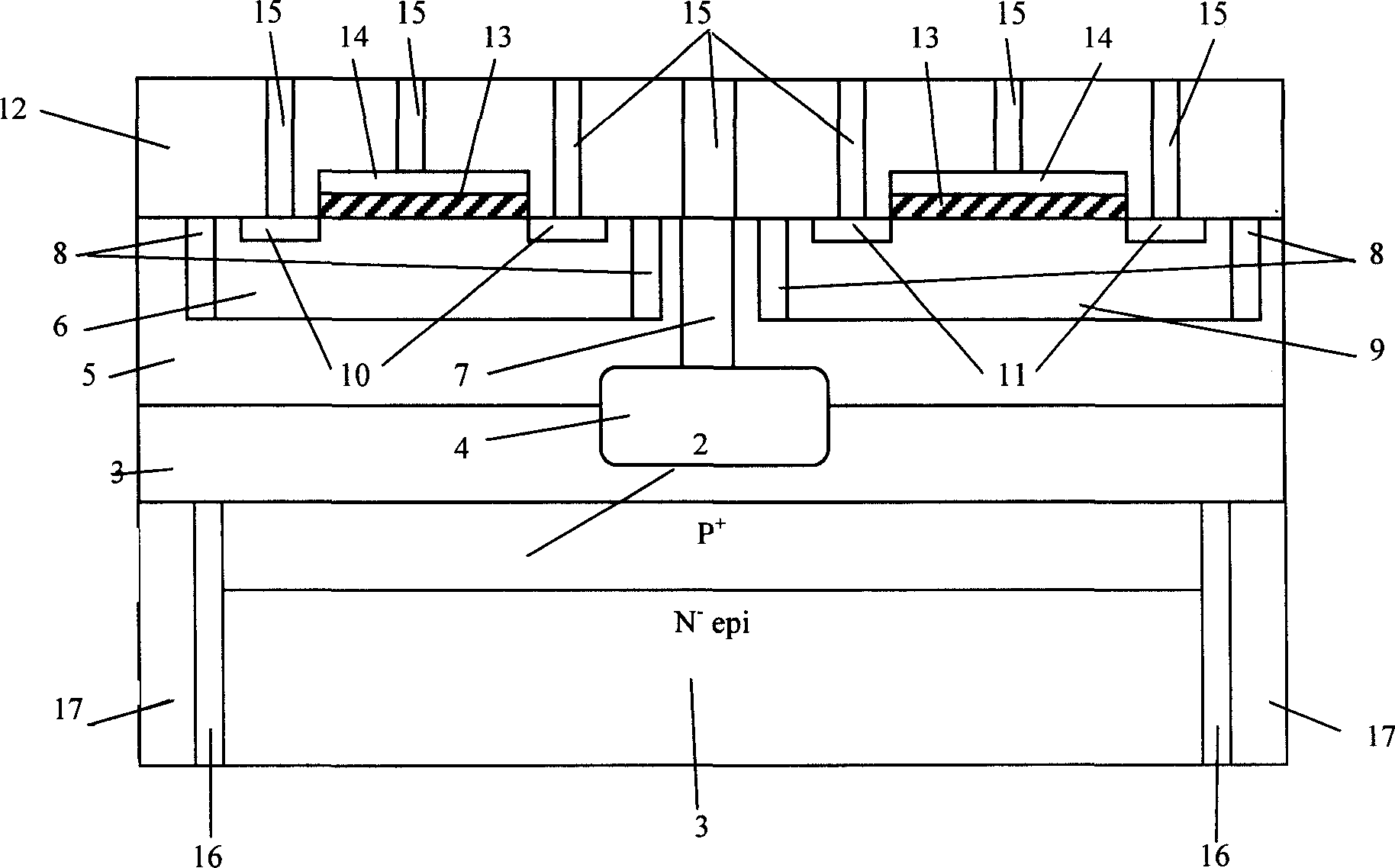
[0051] Specific embodiment two such as figure 1 Shown:

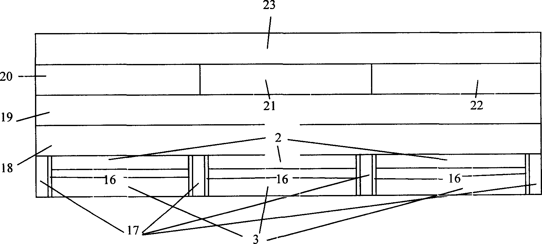
[0052] If the color pixel is different from the first embodiment, the silicon base is different from the upper structure of the P+ layer 2, and an ethyl silicate TEOS layer 18 and a silicon nitride SiN layer 19 can also be arranged in sequence on the P+ layer 2; A blue filter BCF layer 20 , a red filter RCF layer 21 and a green filter GCF layer 22 are arranged on the SiN layer; a photoresist PR layer 23 is arranged on the top.

[0053] The specific implementation manner of the process flow of the manufacturing method of the active pixel image sensor structure with high fill factor of the present invention is as follows, taking Embodiment 1 as an example:

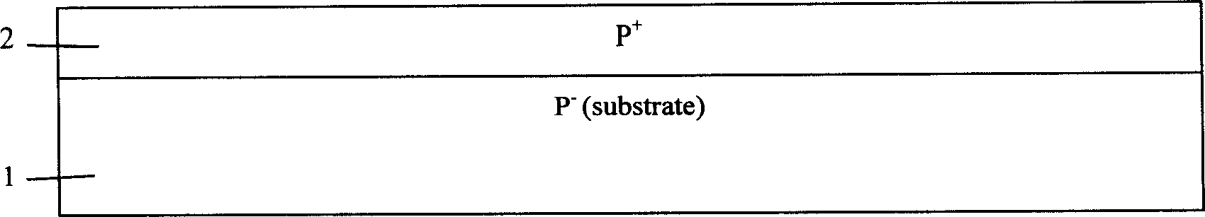
[0054] First, if image 3 As shown, on the P-substrate 1, a layer of SiO was grown by thermal oxygen 2 , with a thickness of 300 angstroms to 350 angstroms. The purpose is to reduce the damage of the P-substrate 1 by ion implantation, and at the same time reduce th...

Embodiment 2

[0060] The specific implementation method of the process flow of the manufacturing method of the active pixel of the second embodiment is as follows: figure 2 Shown on the P+ layer 2 is TEOS[Si(C 2 h 5 o 4 )] 18→SiN19→blue filter layer (BCF) 20→red filter layer (RCF) 21→green filter layer (GCF) 22→photoresist (PR) 23. Because of the high fill factor of this structure, microlenses may not be required.

[0061] The structure of the active pixel structure image sensor of the present invention makes full use of the two sides of the silicon base, wherein the back side is used to manufacture photodiodes for converting incident light into electrical signals, and the front side is used to manufacture signal processing circuits. The filling factor of the entire pixel array is close to 100%, thereby improving the quantum efficiency; and compared with the traditional CMOS image sensor structure, the invented active pixel structure image sensor can obtain a smaller dark area because o...


PUM


Abstract

The present invention relates to high block coefficient active pixel picture sensor structure and manufacturing method. It contains making signal processing circuit on one diode of silica-based support, making photodiode circuit on another side, thereby making block coefficient approaching 100 per cent and maximal raising photodiode structure quantum efficiency. Compared with traditional CMOS picture sensor structure, invented CIS picture sensor has smaller dark current and pixel interference; adopting wet method automatic stop erosion to finely control silicon wafer thinning down thickeness, capable of effectively reducing stress damage, raising sensitivity and block coefficient, and basically solving block coefficient low shortage.

Description

technical field [0001] The invention relates to the technical field of integrated circuit design of microelectronics, in particular to a high filling factor active pixel image sensor structure and a manufacturing method. Background technique [0002] CMOS (Complementary Metal-Oxide-Semiconductor Transistor, Chinese: Complementary Subordinate Oxide Semiconductor) solid-state image sensing technology mainly uses the photoelectric effect characteristics of silicon semiconductor materials. When the silicon semiconductor is in the intrinsic state, the valence band is filled with electrons. The conduction band is filled with holes. When incident light enters a semiconductor, photons are absorbed to generate electron-hole pairs, the necessary condition is that the photons can provide at least the bandgap energy E of silicon g , allowing electrons to jump from the valence band to the conduction band. An incident photon requires at least a bandgap energy E g Electrons can be excit...

Claims


Application Information

Patent Timeline
Patent Type & Authority Applications(China)
IPC IPC(8): H01L27/146H01L21/82
Inventor 金湘亮
Owner BEIJING SUPERPIX MICRO TECHNOLOGY CO LTD
Why Eureka
Try Eureka