Porous silicon light-emitting device
A light-emitting device, porous silicon technology, applied in the field of integrated optoelectronics, can solve the problem of low luminous efficiency of porous silicon materials, and achieve the effects of improving internal quantum efficiency and improving luminous efficiency
- Summary
- Abstract
- Description
- Claims
- Application Information
AI Technical Summary
Problems solved by technology
Method used
Image
Examples
Embodiment 1
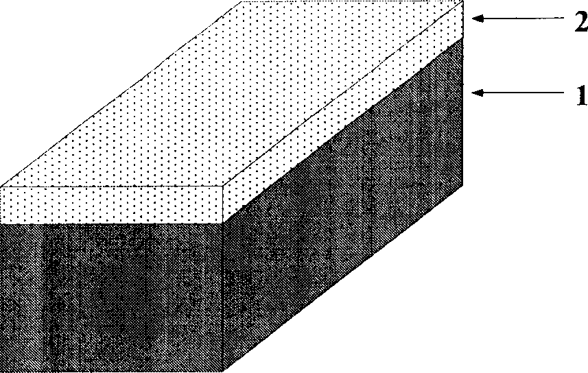
[0028] The basic structure of the porous silicon light-emitting device with metal surface plasmon waveguide of the present invention is as follows Figure 5 shown. Select N, resistivity2 h 5 o 2 =3:7, the current density is 4.4mA / cm 2 , forming a porous silicon layer 1 on a silicon substrate 2 . Afterwards, half of the silicon wafer was covered with tin foil, and the other half was sputtered with a magnetron sputtering station to form a 60nm thick gold film. Then remove the tin foil, and use 514nm laser 11 to irradiate respectively on the porous silicon and the gold film after being focused by the lens 10, and the photoluminescence spectra are respectively as follows Image 6 As shown in 13 and 14, it can be seen that the metal surface plasmon waveguide greatly enhances the photoluminescence of porous silicon.
Embodiment 2
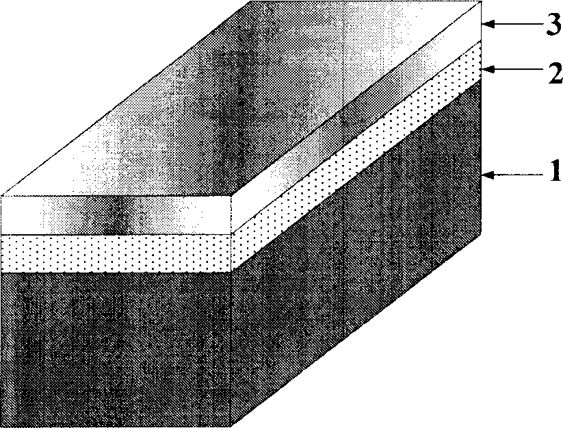
[0030] The basic structure of the porous silicon light-emitting device with metal-dielectric surface plasmon waveguide of the present invention is as follows Figure 7 shown. Select N, resistivity2 h 5 o 2 =3:7, the current density is 4.4mA / cmy, and the porous silicon layer 1 is formed on the silicon substrate 2. Then cover half of the silicon wafer with tin foil, and the other half is sputtered on it with a magnetron sputtering table to form a 60nm thick gold and SiO 2 Blend film. Then remove the tin foil, and use 514nm laser light 11 to irradiate respectively on porous silicon and gold and SiO after focusing through lens 10 2 mixed film.
Embodiment 3
[0032] The basic structure of the porous silicon light-emitting device with metal-dielectric surface plasmon waveguide of the present invention is as follows Figure 7 shown. Select N, resistivity2 h 5 o 2 =3:7, the current density is 4.4mA / cm 2 , forming a porous silicon layer 1 on a silicon substrate 2 . Afterwards, half of the silicon wafer was covered with tin foil, and the other half was sputtered on it using a magnetron sputtering station to form a 60nm-thick mixed film of gold and silver. The tin foil was then removed, and the samples were placed in nitric acid to remove the silver and form porous gold. And use the 514nm laser 11 to focus on the porous silicon and the porous gold film respectively after being focused by the lens 10 .
PUM
| Property | Measurement | Unit |
|---|---|---|
| Thickness | aaaaa | aaaaa |
| Particle size | aaaaa | aaaaa |
| Current density | aaaaa | aaaaa |
Abstract
Description
Claims
Application Information


