

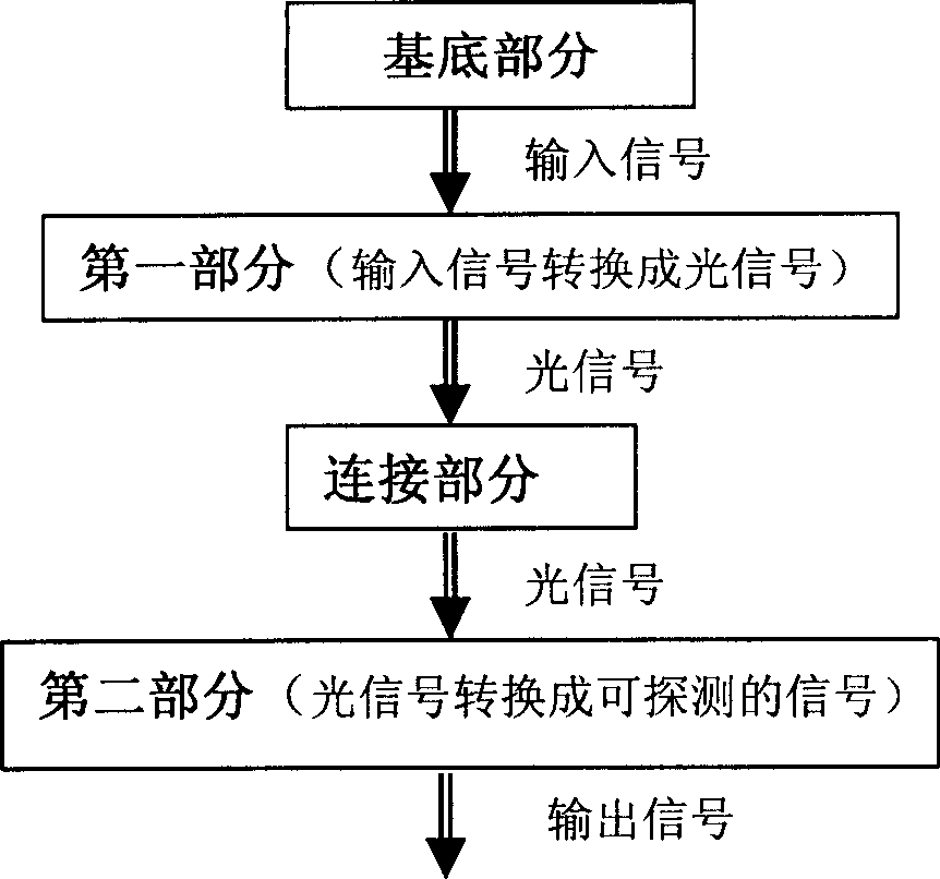
Organic light-coupling device
An optocoupler device, an organic technology, applied in the field of optoelectronics, achieves the effects of simple preparation process, broad application prospects, and cost reduction
- Summary
- Abstract
- Description
- Claims
- Application Information
AI Technical Summary
Problems solved by technology
Method used
Image

Examples
Embodiment 1
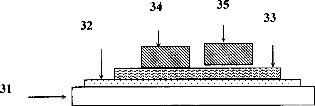
[0043] Prepare an organic optocoupler device that combines an organic electroluminescent display (OLED) and a pentacene photoresistor. The schematic diagram of its structure and its symbols are shown in the attached Figure 5 51 is a glass substrate, 52 is an OLED device, 53 is a pentacene photoresistor device, and 54 is a circuit symbol of the organic optocoupler.
[0044] The manufacturing process steps of the organic optocoupler device are as follows: first, an OLED device 52 is prepared on a glass substrate 51 , and then a pentacene photoresistive device 53 is prepared on the other side of the glass substrate 51 .
[0045] First, prepare a layer of transparent indium tin oxide (ITO) conductive film on the glass substrate, and use the method of photolithography to prepare the ITO into the required pattern as the anode of the OLED; Deposit 100nm copper phthalocyanine on CuPc as a hole carrier injection buffer layer; then use vacuum evaporation method to deposit 20nm NPB hole...
Embodiment 2
[0049] An organic optocoupler device combining an organic electroluminescent display (OLED) and an organic photodiode is prepared. The preparation process steps of the organic photocoupler device are as follows: firstly, an OLED device is prepared on a substrate, and then an organic photosensitive diode is prepared on the other side of the substrate.
[0050] The preparation method of the OLED device can refer to Example 1, except that the material of the base part is polyimide, the materials and preparation process of other parts are the same as in Example 1. Organic photodiodes can have three structural options, and their preparation methods are as follows:
[0051] (a): A preparation method of a p-n junction photodiode is as follows: a thin layer of transparent gold electrode is formed by vapor deposition on the other side of the polyimide as a common substrate, with a thickness of 5nm, which is used as a photodiode. lead electrode, then evaporate and deposit p-type semico...
Embodiment 3
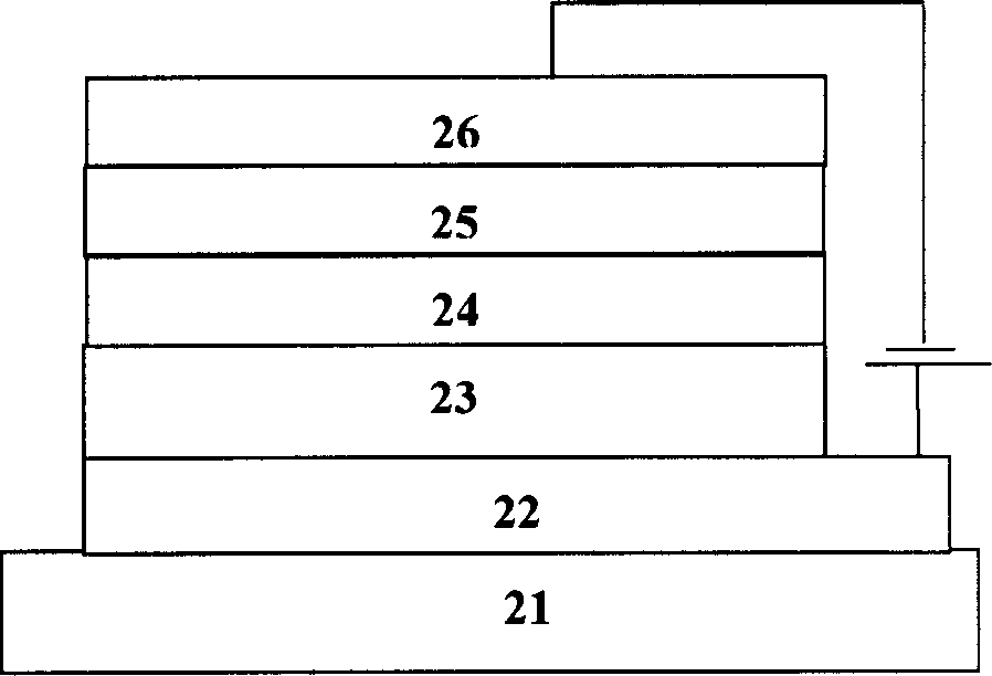
[0056] An organic optocoupler device combining an organic electroluminescent display (OLED) and an organic phototransistor is prepared. The preparation process steps of the organic optocoupler device are as follows: first, a ceramic sheet is used as a substrate, an OLED device is prepared on it, and then an organic photosensitive transistor is continuously prepared on the top of the OLED device.
[0057] The preparation method of OLED device can refer to embodiment 1, and the material of its base part adopts ceramic sheet, and its anode material adopts 15-200nm Ag vacuum evaporation to prepare, and its cathode material adopts 20nm Mg:Ag evaporation to prepare , the materials and preparation process of other parts are all the same as in Example 1.
[0058] A preparation method of an organic photosensitive transistor includes: forming a layer of 30nm polyester film on the top transparent metal electrode of an organic electroluminescent device, and then vapor-depositing a 10nm IT...
PUM
| Property | Measurement | Unit |
|---|---|---|
| Thickness | aaaaa | aaaaa |
| Thickness | aaaaa | aaaaa |
| Thickness | aaaaa | aaaaa |
Abstract
Description
Claims
Application Information