Method for producing heavy blended gallium nitride field effect transistor

A gallium nitride field and heavy doping technology, which is applied in semiconductor/solid-state device manufacturing, electrical components, circuits, etc., can solve the problems that the doping amount cannot be increased, the output power cannot be increased, and the performance cannot be improved. Current collapse, increase output power, reduce the effect of current collapse

Inactive Publication Date: 2007-01-24
NO 55 INST CHINA ELECTRONIC SCI & TECHNOLOGYGROUP CO LTD
View PDF0 Cites 5 Cited by
  • Summary
  • Abstract
  • Description
  • Claims
  • Application Information

AI Technical Summary

Problems solved by technology

[0008] The purpose of the present invention is to solve the problem that the performance of the existing GaN field effect transistor cannot be improved due to the inability to increase the doping amount, and to invent a method that can not only heavily dope the GaN field effect transistor, but also not A method of fabricating heavily doped eGaN field effect transistors that can significantly increase output power due to the common current collapse phenomenon caused by heavy doping

Method used


Image

  • Method for producing heavy blended gallium nitride field effect transistor
  • Method for producing heavy blended gallium nitride field effect transistor
  • Method for producing heavy blended gallium nitride field effect transistor

Examples


specific manufacture example 1

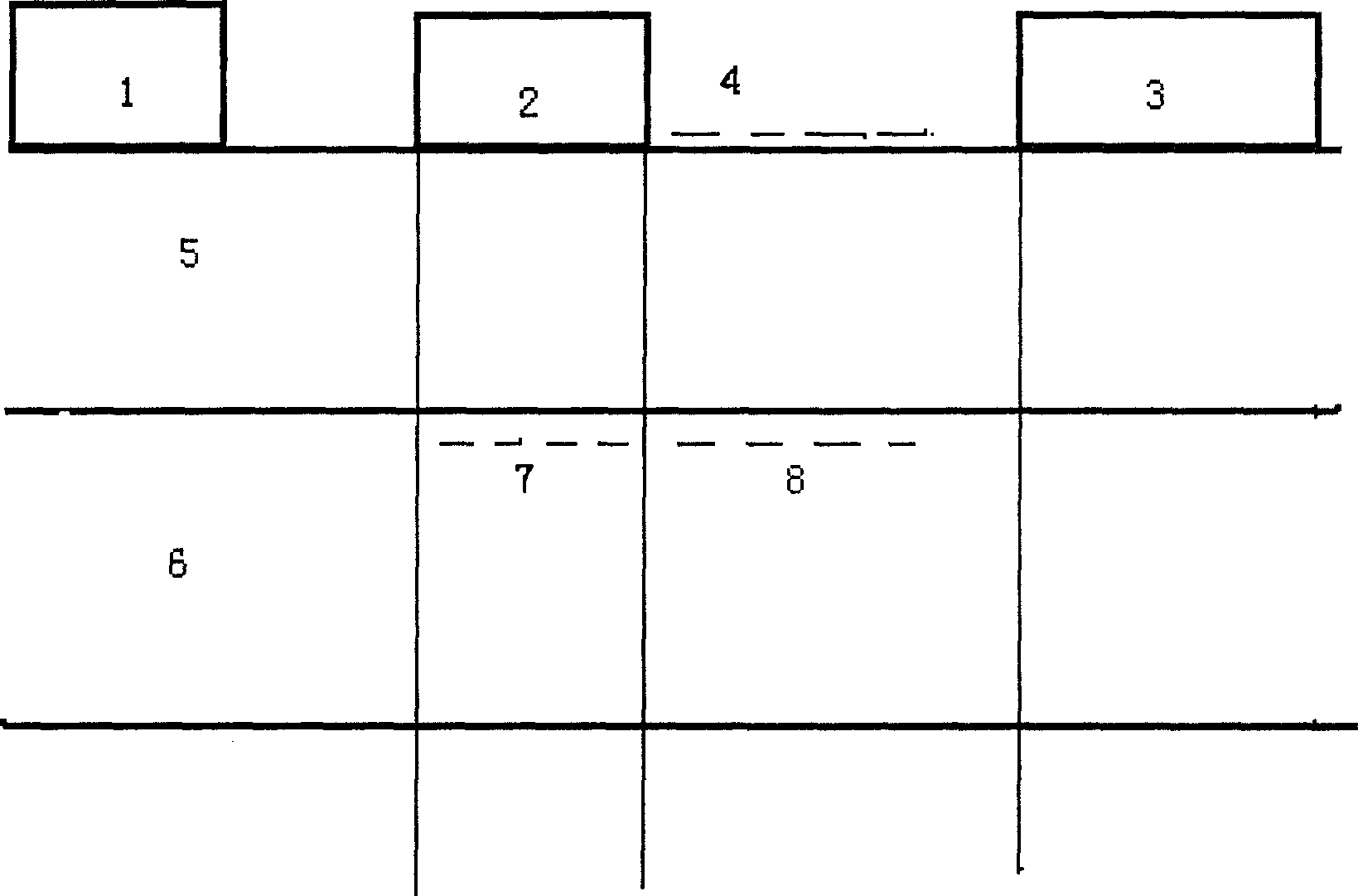
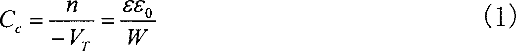
[0031] Specific manufacturing example 1: Take the thickness d of the cap layer 7 =2nm, doped layer thickness d 6 =20nm, the doping concentration is 10 19 cm -3 , isolation layer thickness d 5 =1nm, the Al composition ratio of the barrier layer is 0.3. Self-consistently solving the Schrödinger equation and Poisson equation, the electron gas density when the barrier layer is doped and undoped is 2.27*10 respectively 13 / cm 2 and 1.24*10 13 / cm 2 . The pinch-off voltages calculated by formula (2) are -10.1V and -5.5V, respectively. When there is no doping, the pinch-off voltage just meets the above nW rule, and the channel can be pinched off normally. For the doping barrier, use fluorine plasma treatment (control the plasma emission power between 100-150W, and the treatment time is between 120-180 seconds) to increase the inner channel barrier by 5V, then the pinch-off of the inner channel The voltage is -5.1V. It also meets the nW rule and can be pinched off normally....

specific manufacture example 3

[0033] Specific manufacturing example 3: When the Al composition ratio is lower, the electron gas density decreases, and the thickness W of the barrier layer can be appropriately increased to increase the electron gas density. Take the Al composition ratio as 0.2, and the doped layer thickness d 6 =25nm, the doping concentration is 8*10 18 cm -3 . At this time, the electron gas density when the barrier layer is doped and undoped is 1.81*10 13 / cm 2 and 7.88*10 12 / cm 2 . The pinch-off voltages calculated by formula (2) are -9.82V and -4.27V, respectively. The undoped pinch-off voltage of -4.27V also complies with the above nW rule, and the channel can be pinched off normally. After the barrier layer is doped, use fluorine plasma treatment (control the plasma emission power between 100-150W, and the treatment time is between 120-180 seconds) to increase the inner channel barrier by 5V, then the clamping of the inner channel The cut-off voltage is -4.82V. Also within t...


PUM


Abstract

This invention provides a method for manufacturing heavy doped GaN field effect transistors including: growing a nucleation layer, a buffer layer and a channel layer on a substrate, then growing an AlN isolation layer and a heavy doped AlGaN potential barrier layer and finally making mesa-isolation and ohm contact to photo-etch a grating electrode window after growing a non-doped cap layer then to be processed by CF4 fluorin plasma process to control the emission power and process time to adjust the pinch off voltage to a designed sphere, then self-aligning the deposited grating metal on the barrier layer of the window to manufacture the Schottky barrier and annealing in the N2 atmosphere to eliminate defect generated in the plasma process to get the heavy doped field effect transistor.

Description

technical field [0001] The invention relates to a method for manufacturing a semiconductor device, in particular to a method for manufacturing a heavily doped variable barrier gallium nitride field effect transistor, in particular to a method for manufacturing a heavily doped gallium nitride field effect transistor. Background technique [0002] The GaAs HFET is doped in the barrier layer, and the electrons generated by ionization of impurities are transferred to the channel to form a two-dimensional electron gas, which achieves good radio frequency performance. This modulating doping method was transplanted into GaN HFETs, and the devices studied earlier were all doped in the barrier layer. However, nitride is a polar semiconductor, and there are strong polarized charges and large energy band steps at the AlGaN / GaN heterointerface. The barrier layer can be produced without doping 10 13 / cm 2 order of magnitude high electron gas density. Whether it is necessary to dope t...

Claims


Application Information

Patent Timeline
IPC IPC(8): H01L21/335
Inventor 薛舫时
Owner NO 55 INST CHINA ELECTRONIC SCI & TECHNOLOGYGROUP CO LTD
Why Eureka
Try Eureka