Method for preparing p type copper sulfide transparent conducting film

A technology of transparent conductive film and copper sulfide, which is applied in semiconductor/solid-state device manufacturing, circuits, electrical components, etc., can solve the problems of low conductivity and transmittance of p-type film, difficult precise control of composition, complicated preparation process, etc. Achieve the effect of smooth and bright surface, low manufacturing cost and simple preparation process

Inactive Publication Date: 2007-04-18
SHANGHAI INST OF CERAMIC CHEM & TECH CHINESE ACAD OF SCI
View PDF0 Cites 10 Cited by
  • Summary
  • Abstract
  • Description
  • Claims
  • Application Information

AI Technical Summary

Problems solved by technology

[0005] The object of the present invention is to provide a kind of p-type copper sulfide Cu x The preparation method of S (x is between 1-2) transparent conductive thin films realizes p-type thin film materials with superior electrical conductivity and high transmittance in the visible light range, and the preparation process is simple and easy to operate, overcoming the conductivity of common p-type thin films and low transmittance, complex preparation process, high cost, harsh conditions and difficult to precisely control the composition

Method used


Image

  • Method for preparing p type copper sulfide transparent conducting film
  • Method for preparing p type copper sulfide transparent conducting film
  • Method for preparing p type copper sulfide transparent conducting film

Examples


Embodiment 1

[0024] (1) Using quartz glass as the substrate (glass sheet or glass tube), place the substrate in deionized water, absolute ethanol and acetone solvents for 10 minutes and ultrasonically clean it for 10 minutes to remove the grease and dirt on the surface. Then it was dried in a vacuum oven at 100°C for use.

[0025] (2) Add 0.5 g of 3-amino-propyl-trimethoxysilane dropwise into a mixed solution of 15 ml of absolute ethanol and 5 ml of deionized water, then add 0.05 g of acetic acid, and stir for 15 min. Put the cleaned substrate into the above solution, take it out after standing for 48 hours, wash it with deionized water to remove excess physically adsorbed silane molecules, make the surface of quartz glass self-assemble to form a silane monomolecular film, and dry it in vacuum at 100°C for 30 minutes .

[0026] (3) 0.3157g CuCl 2 2H 2 Dissolve O in 20ml of deionized water, add 1.48ml of triethanolamine, and mix well; then add 2.96ml of NH 4 OH; finally add 50ml of 0.02...

Embodiment 2

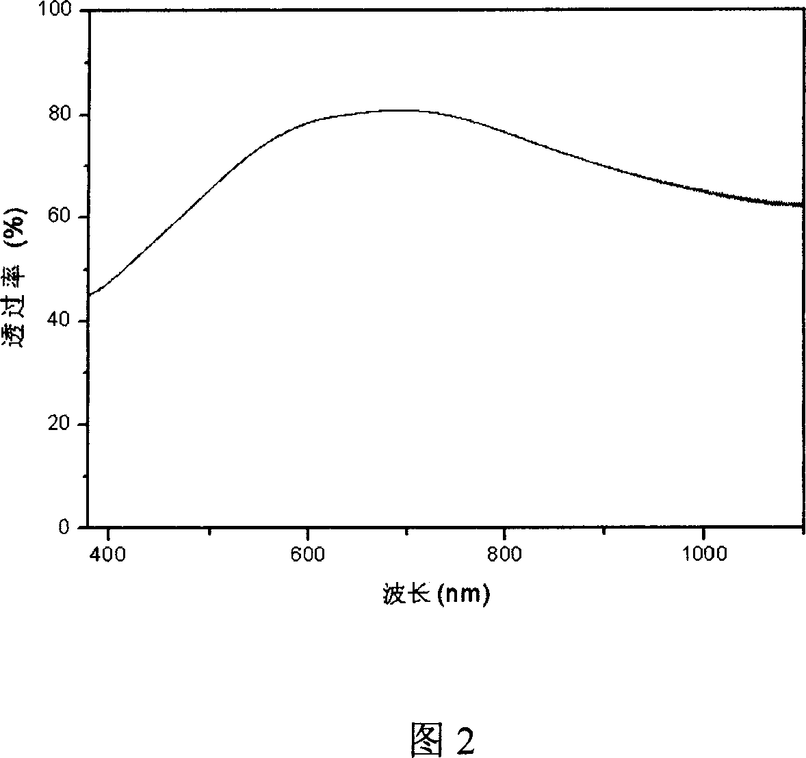
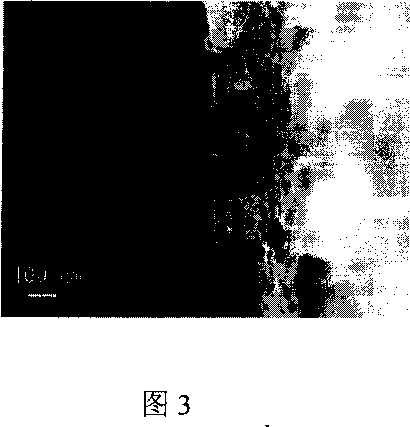
[0030] The cleaning of the quartz glass substrate and the preparation of the monomolecular film are the same as in Example 1. The preparation of the precursor solution adopts the following composition: 20ml of 0.1mol / l CuSO 4 , 3.5ml Thioacetamide, 5ml NH4 OH and 40ml of 0.04mol / l (NH 3 ) 2 CS solution. Submerge the substrate in the precursor solution and seal the container. Then put it into a water bath, control the temperature at 60±1°C, take out the film after 3 hours of nucleation and growth, wash it with deionized water and dry it naturally. The thickness of the film prepared under this condition is 77nm, and the chemical composition is Cu 1.82 S. The SEM photos of the film surface and cross-section are shown in Figure 3 and Figure 4, respectively. It can be seen that the film is uniform and continuous, and the surface is flat. Illustrate the Cu prepared by this example x S film is a transparent conductor with high appearance quality.

Embodiment 3

[0032] Using 3-mercapto-propyl-trimethoxysilane instead of 3-amino-propyl-trimethoxysilane in Example 1, the cleaning of the quartz glass substrate and the preparation process of the monomolecular film are the same as in Example 1. The preparation of the precursor solution is the same as in Example 2, the growth temperature of the film is 50±1° C., the growth time is 2 hours, and the rest of the process steps are the same as in Example 1. The transmittance of the film is equivalent to that of Example 1, and the relationship of the electrical conductivity with temperature is shown in FIG. 5 . As the temperature increases, the conductivity of the film increases, showing semiconducting properties.


PUM

PropertyMeasurementUnit
thicknessaaaaaaaaaa
thicknessaaaaaaaaaa
electrical conductivityaaaaaaaaaa

Abstract

The invention relates to a p-type copper sulphide transparent conductive film preparing method, characterized in forming unimolecular film on transparent quartz glass substrate surface by silicane molecule chemical absorption, and then diping in the prepared precursor solution. By induction of the unimolecular film, by controlling growth temperature and time of the film and the proportions of components of the precursor solution, it can prepare films of different conductivities and transmittances. At room temperature, the conductivity of the film can reach above 105S/m, average transmittance of the film in visible light range reaches above 60% and the transmittance of the film in local range can reach above 80%. And it can prepare films on substrates with complex shapes, suitable for industrialized large area film production. And the prepared p-type CuxS transparent conductive film can be applied to flat panel displays, solar batteries, LEDs and other photoelectric devices.

Description

technical field [0001] The invention relates to a p-type copper sulfide Cu x The preparation method of S (x is between 1-2) transparent conductive film, specifically utilizes monomolecular membrane assisting method to prepare Cu with high conductivity and high transmittance x The invention relates to an S thin film, which belongs to the technical field of thin film material preparation. Background technique [0002] Transparent conductive film with good conductivity and high light transmittance in the visible spectrum region, widely used in liquid crystal displays, solar cells, touch panels, special function window coatings and other optoelectronic devices. So far, the transparent conductive films put into practical application are mainly n-type semiconductor films, such as transparent conductive tin-doped indium oxide (ITO), fluorine-doped tin oxide (FTO), aluminum-doped zinc oxide (AZO), etc. With the rapid development of optoelectronic devices, more and more occasions r...

Claims


Application Information

Patent Timeline
Patent Type & Authority Applications(China)
IPC IPC(8): H01L31/18H01L33/00H01L21/288H01L21/3205C23C18/00
CPCY02P70/50
Inventor 刘付胜聪陈立东
Owner SHANGHAI INST OF CERAMIC CHEM & TECH CHINESE ACAD OF SCI
Why Eureka
Try Eureka