
Grating element and external resonator type light emitting device

a light emitting device and grating element technology, applied in the direction of optical elements, semiconductor lasers, instruments, etc., can solve problems such as optical intensity change, and achieve the effects of reducing optical power fluctuations, enhancing wavelength stability, and increasing the tolerance of axial misalignmen

Active Publication Date: 2018-09-11
NGK INSULATORS LTD
View PDF23 Cites 0 Cited by
  • Summary
  • Abstract
  • Description
  • Claims
  • Application Information

AI Technical Summary

Benefits of technology

The solution achieves stable wavelength operation with reduced temperature dependency and optical power fluctuations, allowing for compact design without additional temperature control elements, and increased tolerance to axial misalignment, thereby improving the reliability and efficiency of the laser module.

Problems solved by technology

In particular, as current or temperature changes, the lasing wavelength of the laser varies, which results in a change in the optical intensity.

Method used


Image

  • Grating element and external resonator type light emitting device
  • Grating element and external resonator type light emitting device
  • Grating element and external resonator type light emitting device

Examples


example 1

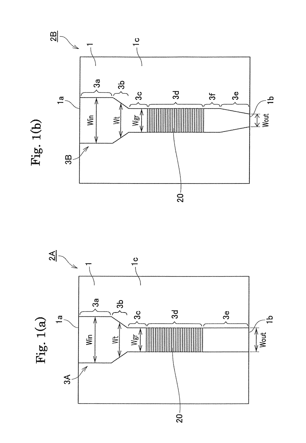
[0202]Grating elements shown in FIGS. 1(a), 2 and 4 was fabricated in the following way.

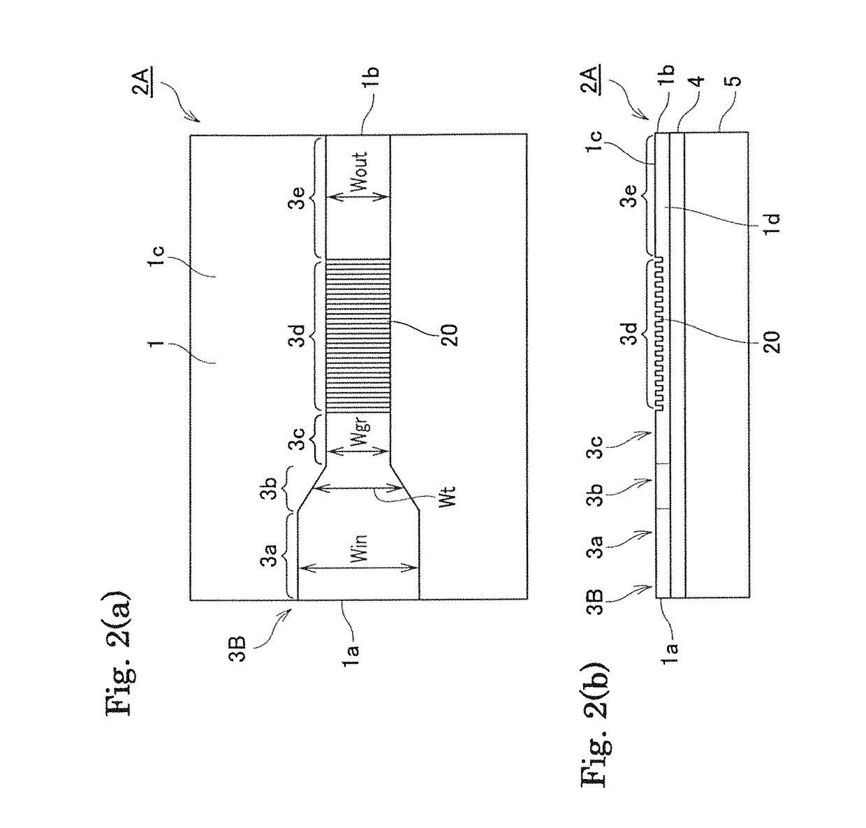
[0203]Specifically, SiO2 was deposited in a thickness of 1 μm by a sputtering device on a support substrate 5 made of quartz, and Ta2O5 was deposited thereon in a thickness of 2 μm to form an optical material layer 1. Then, Ti was deposited on the optical material layer 1, and a grating pattern was fabricated by the photolithography technique.

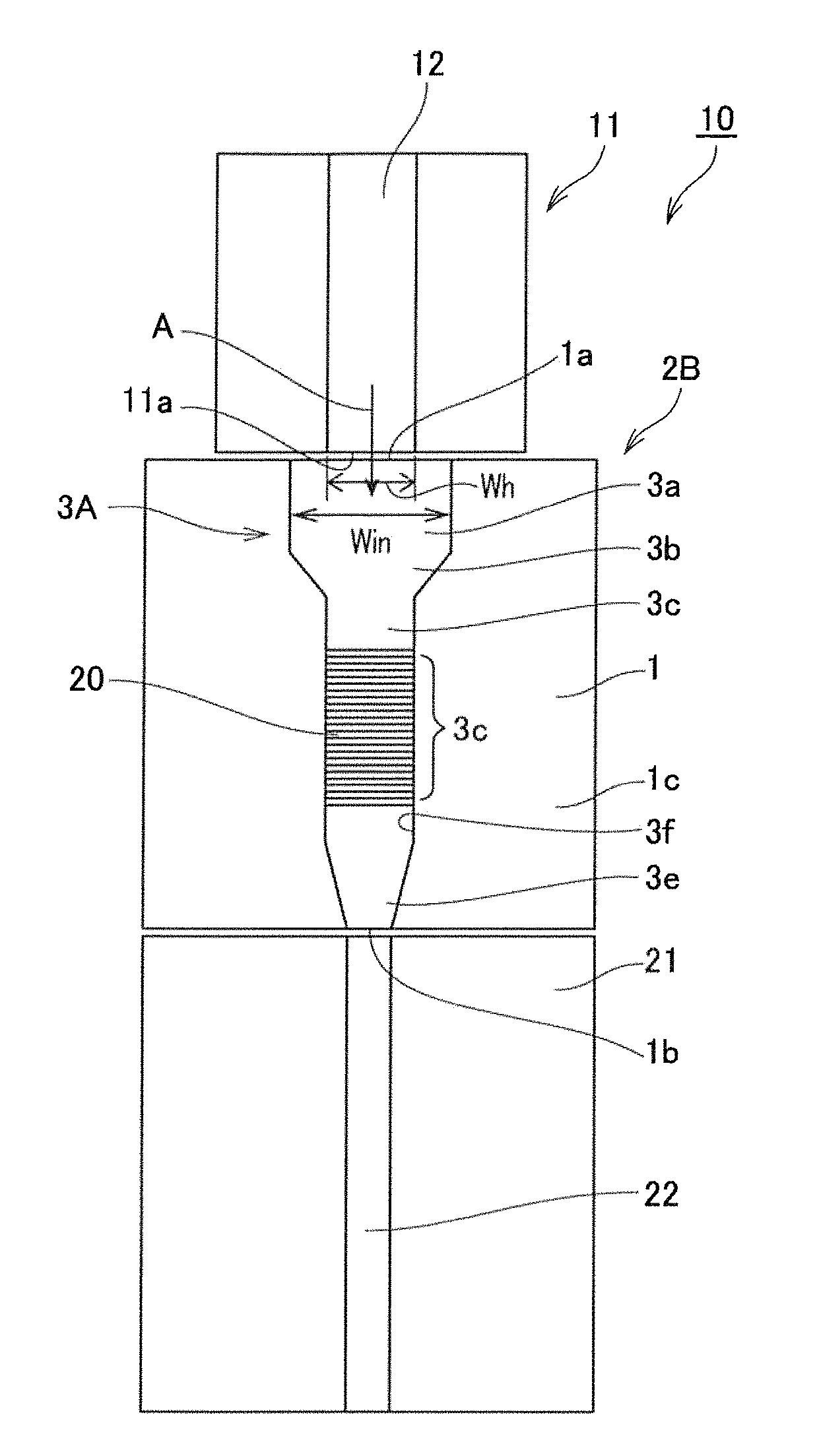
[0204]Thereafter, grating grooves were formed at a pitch interval Λ of 205.4 nm with a length Lb of 25 μm by fluorine reactive ion etching using the Ti pattern as a mask. The groove depth td of the grating was set to 100 nm. Further, a waveguide was patterned by the photolithography technique to form a pattern therein, and a ridge groove process was performed by reactive ion etching to form the incident portion with the width Win of 8 μm and the thickness Tr of 1 μm as well as the grating portion with the width Wgr of 3 μm and the thickness Tr of 1 μm. The l...

example 2

[0238]A grating element having the same structure was formed in the same way as in Example 1. However, a ridge groove process was performed to form the light-source input portion with the width Win of 8 μm and the thickness Tr of 1 μm as well as the grating portion with the width Wgr of 2 μm and the thickness Tr of 1 μm. The length from the input end face to the starting point of the grating portion was set at 25 μm.

[0239]Thereafter, the input side and output side of the element were etched down to the quartz substrate by dry etching to thereby make mirror surfaces at end faces thereof. Finally, SiO2 was formed by sputtering to form a single-layer film of 90 nm in thickness at both end faces. At this time, the reflectance of the end face was 3%. The element size was set to have 1 mm width and 100 μm length Lwg.

[0240]Regarding the optical characteristics of the grating element, the reflection characteristics of the grating element were evaluated from the transmission characteristics ...

example 3

[0254]Elements shown in FIGS. 1 (a) and 3 were fabricated in the following way.

[0255]Specifically, SiO2 was deposited in a thickness of 2 μm by a sputtering device on a support substrate 5 made of quartz, and Ta2O5 was deposited thereon in a thickness of 2 μm to thereby form an optical material layer 1. Then, Ti was deposited on the optical material layer 1, and a grating pattern was fabricated by the photolithography technique. Thereafter, grating grooves were formed at a pitch interval Λ of 205.4 nm with a length Lb of 25 μm by the fluorine reactive ion etching using the Ti pattern as a mask. The groove depth td of the grating was set to 100 nm. Further, a waveguide was patterned by the photolithography technique to form a pattern therein, and a ridge groove process was performed by the reactive ion etching to form the incident portion with the width Win of 8 μm and the thickness Tr of 1.6 μm as well as the grating portion with the width Wgr of 3 μm and the thickness Tr of 1.6 μm....


PUM


Abstract

A grating element includes: a support substrate; an optical material layer; a ridge optical waveguide having an incidence surface on which a laser light is incident and an emission end from which an emission light with a desired wavelength is emitted; and a Bragg grating including concave and convex portions formed within the optical waveguide. The optical waveguide includes an incident portion between the incidence surface and the Bragg grating, and a tapered portion between the incident portion and the Bragg grating. In the Bragg grating, a propagation light propagates in single mode. The width Win of the optical waveguide in the incident portion is larger than the width Wgr of the optical waveguide in the Bragg grating. The width Wt of the optical waveguide in the tapered portion is decreased from the incident portion toward the Bragg grating. The relationships represented by formulas (1) to (3) are satisfied.

Description

TECHNICAL FIELD[0001]The present invention relates to a grating element and an external resonator type light emitting device using the same.BACKGROUND ARTS[0002]Semiconductor lasers generally used are of a Fabry-Perot (FP) type that includes an optical resonator sandwiched between mirrors formed at both end faces of an active layer. However, the FP laser oscillates at a wavelength that satisfies the standing-wave condition, and thereby tends to operate in a multi-longitudinal mode. In particular, as current or temperature changes, the lasing wavelength of the laser varies, which results in a change in the optical intensity.[0003]Meanwhile, for the purpose of optical communications, gas sensing, and the like, lasers are required to exhibit high wavelength stability and to oscillate in a single mode. For this reason, a distributed feedback (DFB) laser and a distributed Bragg reflector (DBR) laser have been developed. These lasers are designed to include a diffraction grating formed in...

Claims


Application Information

Patent Timeline
Patent Type & Authority Patents(United States)
IPC IPC(8): H01S5/14G02B6/30G02B6/124G02B6/122G02B6/42G02B6/12
CPCH01S5/141G02B6/122G02B6/124G02B6/12019G02B6/305G02B6/42G02B6/12016G02B6/1228
Inventor KONDO, JUNGOYAMAGUCHI, SHOICHIROASAI, KEIICHIROEJIRI, TETSUYAOKADA, NAOTAKE
Owner NGK INSULATORS LTD
Learn More