Multilayer flexible planar embedded laminated electrode and manufacturing method and application thereof

a flexible, laminated electrode technology, applied in the field of organic electronic devices, can solve the problems of limiting the size of the crystal, the degree of device integration is lower, and the loss of the organic semiconductor field effect performance, etc., to achieve high integration, high precision and complex patterns, and high photolithography techniques.

Active Publication Date: 2018-11-20
NORTHEAST NORMAL UNIVERSITY
View PDF13 Cites 0 Cited by
  • Summary
  • Abstract
  • Description
  • Claims
  • Application Information

AI Technical Summary

Benefits of technology

[0004]The purpose of the present invention is to provide a multilayer flexible planar embedded laminated electrode and manufacturing method and the application thereof in the organic single-crystal field effect transistor, and the method provided by the present invention can be operated at room temperature, and thus in turn avoiding the pollution and damage from the solution and radiation to organic semiconductors; an electrode structure provided the present invention is a planar embedded electrode, namely the electrode and the insulating layer are in the same plane, which ensure that the organic semiconductor and the electrode and the insulating layer are completely fit to obtain high performance devices; and having high integration, complex patterns can be manufactured; can be reusable, and suitable to organic single crystals with various sizes.
[0028]The present invention manufactures the multilayer flexible planar embedded laminated electrode, of which electrode structure is embedded electrode that the electrode and insulating layer are in the same planar and is flexible, and enables the electrode, the insulating layer and organic crystal to completely contact, thus, organic single crystals field-effect transistor of high-performance can be manufactured; manufacturing method provided by the present invention can be operated at room temperature, and the organic semiconductor does not experience the damage to the radiation, the developer and the stripping liquid; the manufacturing method manufactures the electrode by using high precise photolithography technique, and high precise and complex patterns can be manufactured, thus, high integration and convenient and practical can be achieved; because the flexibility of the PDMS and the metal itself is very well, the electrode, the insulating layer and the substrate are flexible, thus, the manufacturation of full flexible devices can be implemented; because the semiconductor and the electrode and the insulating layer are bonded together by the function of the electrostatic adsorption, the electrode can be reused; such flexible planar embedded laminated electrode is suitable to organic single crystal with various sizes.

Problems solved by technology

If using conventional methods (the vacuum deposition mask method) to directly construct electrodes on the organic semiconductor and manufacture a field effect transistor, an organic semiconductor will suffer thermal radiation injury, etc, seriously cause loss of the organic semiconductor field effect performance (Advanced Materials 2008, 20, 2947; Advanced Materials 2008, 20, 1511).
But the disadvantage of this approach is that probe station operation is required to be used, which requires fine operation and is suitable for manufacturing a single device, and the degree of device integration is lower; device with bottom-gate top-contact configuration is suited for organic micro / nano-crystals, but not suitable for larger (>100 microns) crystals, which limit size for use of the crystal.
However, both methods have a common disadvantage that in the electrode structure manufactured by them as shown in FIG. 1, the source / drain electrodes are protruding from the surface of the insulating layer, thus such structure is more suitable for larger size of crystal and a wider channel length, and also limits the use size of the crystal and device to be small.
Because when the organic micro / nano semiconductor is transferred onto such electrode structure, as shown in FIG. 2, this structure, of which electrode is projected, will lead organic semiconductor can not be completely fit with the insulating layer, and the air gap can be very easily formed near the electrodes.
Therefore, this will lead to non-uniform of conduction channel of device and affect the performance of the device.

Method used


Image

  • Multilayer flexible planar embedded laminated electrode and manufacturing method and application thereof
  • Multilayer flexible planar embedded laminated electrode and manufacturing method and application thereof
  • Multilayer flexible planar embedded laminated electrode and manufacturing method and application thereof

Examples


embodiment 1

, Manufacturing a Flexible Planar Embedded Laminated Electrode

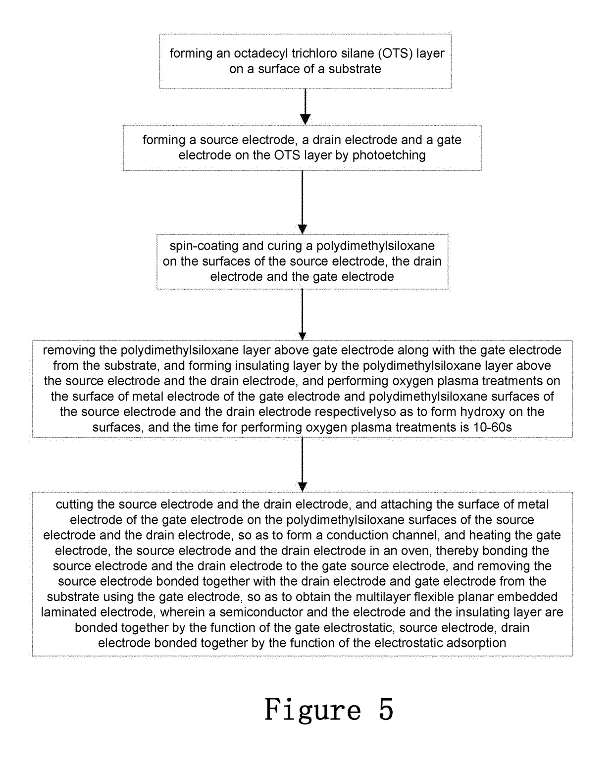
[0044]1. A silicon surface is modified using Octadecyl trichloro silane (OTS): firstly cleaning the surface of the substrate; then placing the substrate in piranha solution (solution of concentrated sulfuric acid and hydrogen peroxide in volume ratio of 7:3), forming hydroxylation at the surface of substrate; cleaning substrate again; placing the substrate OTS solution of n-heptane in volume ratio of 1000:1, enabling the surface of substrate to form a layer of OTS.

[0045]2. A source / drain and the gate electrodes are manufactured on the OTS modified substrates using photolithography method respectively, and mercaptopropyl trimethoxysilane (MPT) may be modified at the surface of the metal surface: firstly, photoetching (baking temperature: 100 degrees; baking time: 3 minutes (min); exposure time: 20 s; developing time: 60 s; fixing time: 30 s) on the substrate using AZ5214E photoresist; and then vacuum vapor depositing a lay...

embodiment 2

, Manufacturing a Flexible Planar Embedded Laminated Electrode

[0059]1. A glass surface is modified using Octadecyl trichloro silane (OTS): firstly cleaning the surface of the substrate; then placing the substrate in piranha solution (solution of concentrated sulfuric acid and hydrogen peroxide in volume ratio of 7:3), forming hydroxylation at the surface of substrate; cleaning substrate again; placing the substrate OTS solution of n-heptane in volume ratio of 1000:1, enabling the surface of substrate to form a layer of OTS.

[0060]2. A source / drain and the gate electrodes are manufactured on the OTS modified substrates using photolithography method respectively, and mercaptopropyl trimethoxysilane (MPT) may be modified at the surface of the metal surface: firstly, photoetching (baking temperature: 100° C.; baking time: 3 minutes (min); exposure time: 20 s; developing time: 60 s; fixing time: 30 s) on the substrate using AZ5214E photoresist; and then vacuum vapor depositing a layer of ...

embodiment 3

, Manufacturing a Flexible Planar Embedded Laminated Electrode

[0068]1. A glass surface is modified using Octadecyl trichloro silane (OTS): firstly cleaning the surface of the substrate; then placing the substrate in piranha solution (solution of concentrated sulfuric acid and hydrogen peroxide in volume ratio of 7:3), forming hydroxylation at the surface of substrate; cleaning substrate again; placing the substrate OTS solution of n-heptane in volume ratio of 1000:1, enabling the surface of substrate to form a layer of OTS.

[0069]2. A source / drain and the gate electrodes are manufactured on the OTS modified substrates using photolithography method respectively, and mercaptopropyl trimethoxysilane (MPT) may be modified at the surface of the metal surface: firstly, photoetching (baking temperature: 100 degrees; baking time: 3 minutes (min); exposure time: 20 s; developing time: 60 s; fixing time: 30 s) on the substrate using AZ5214E photoresist; and then vacuum vapor depositing a layer...


PUM


Abstract

A flexible planar embedded laminated electrode can be manufactured by a method in which an octadecyl trichloro silane connected on the surface of a substrate; a source electrode, a drain electrode and a gate electrode are manufactured using photoetching; mercaptopropyl trimethoxysilane is connected at surfaces of metal electrodes of the source electrode, the drain electrode and the gate electrode; a polydimethylsiloxane is spin-coated on the respective surfaces for metal electrodes of the above electrodes; the gate electrode spin-coated with polydimethylsiloxane is removed from the substrate; oxygen plasma treatments are performed, so as to form hydroxy on the surfaces; the source electrode and the drain electrode are cut, and the gate electrode, the source electrode and the drain electrode are connected to form an integral to obtain the flexible planar embedded laminated electrode.

Description

CROSS-REFERENCE TO RELATED APPLICATIONS[0001]This application is the U.S. National Phase under 35. U.S.C. § 371 of International Application PCT / CN2015 / 000460, filed Jun. 26, 2015, which claims priority to Chinese Patent Application No. 201410341768.5, filed Jul. 17, 2014. The disclosures of the above-described applications are hereby incorporated by reference in their entirety.TECHNICAL FIELD[0002]The present invention relates to a multilayer flexible planar embedded laminated electrode and manufacturing method and application thereof, which belongs to the field of organic electronic.BACKGROUND[0003]Since the first organic field effect transistor is invented in 1986 (Applied Physics Letters 1986, 49, 1210), because of its feature such as simple manufacturing process, wide range of material sources, low cost and good compatibility with flexible substrates, etc. (Nature 2004, 428, 911; Advanced Materials 2005, 17, 1705; Journal of Materials Chemistry 2005, 15, 53; Advanced Materials ...

Claims


Application Information

Patent Timeline
Patent Type & Authority Patents(United States)
IPC IPC(8): H01L51/10H01L51/00H01L51/05
CPCH01L51/105H01L51/102H01L51/055H01L51/0023H10K71/60H10K10/462H10K10/82H10K10/84H10K71/621H10K10/481
Inventor TONG, YANHONGLIU, YICHUNTANG, QINGXINZHAO, XIAOLI
Owner NORTHEAST NORMAL UNIVERSITY
Why Eureka
Try Eureka