Process of forming a photoactive layer of an optoelectronic device

a technology of optoelectronic devices and photoactive layers, which is applied in the direction of electrophoretic coatings, electrolytic capacitors, liquid/solution decomposition chemical coatings, etc., can solve the problems of difficult large-scale production of these types of pv cells, difficult process of applying photoactive layers,

Active Publication Date: 2018-12-18
COMMONWEALTH SCI & IND RES ORG
View PDF7 Cites 2 Cited by
  • Summary
  • Abstract
  • Description
  • Claims
  • Application Information

AI Technical Summary

Benefits of technology

[0013]The perovskite semiconductor forming the photoactive layer is formed by conversion of a metallic layer of or on the substrate to a perovskite through treatment with a suitable reactive compound, for example acetic acid, halide, organohalide or inorganic halide or combination thereof, such that the metallic surface forms an intermediate compound that can subsequently be converted to the active perovskite material. It should be understood that by metal and metallic the invention relates to the atomic or alloy form of said metal and not an ionic form thereof. By using a metal layer (provided by the substrate as a coating or in the comprising material) and subsequent semiconductor formation, the spatial and scalar uniformity of an optoelectronic device is improved in an economic manner. The use of such a composite electrode material in an optoelectronic device addresses the scalar limitations imposed by existing fabrication processes for perovskite semiconductors. This method can also provide improved energy conversion capabilities.
[0019]In these embodiments, the perovskite semiconductor forming the photoactive layer is formed by deposition of a thin metallic layer on the substrate that is subsequently converted to a perovskite through treatment with a suitable reactive compound, including acetic acid, halide, organohalide or inorganic halide or combination thereof, such that the metallic surface forms an intermediate compound that can subsequently be converted to the active perovskite material. In some embodiments, the direct deposition of a metal such as Pb can result less oxygen present within the final perovskite film, say for example compared to depositing a metal compound, such as PbO.
[0108]It should be appreciated that the present invention can be used to form single junction or multijunction cells. Multi-junction (MJ) solar cells comprise solar cells with multiple p-n junctions, preferably made of different semiconductor materials. Each material's p-n junction will produce electric current in response to different wavelengths of light. Multijunction cells can be produced by layering a series of perovskite layers / structures formed using the process of the present invention. The use of multiple semiconducting materials allows the absorbance of a broader range of wavelengths, improving the cell's sunlight to electrical energy conversion efficiency. Examples of multijunction cells include the use with Si as a tandem structure, but also including multijunction perovskites where a distinct advantage of electrodeposited or vapour deposited embodiments is the ability to form multi-layered stacks of thin-films over large areas. In this respect, quantification of the spectral band edge of perovskite materials of varying composition. For example, in some embodiments, successive layers of a halide series from I, Cl, Br etc. would enable spectral tuning of the device and lead to a broader spectral response and higher efficiency. In some embodiments, the present invention is used to deposit a perovskite material with a suitable and complementary band gap would enable a broader spectral response of existing semiconductor photovoltaics, for example deposition of CH3NH3PbI3 as a top-cell on silicon to form a tandem junction.
[0139]Finally, it is noted that preferred embodiments of the optoelectronic device of the present invention will be produced without a porous TiO2 film. This has two advantages:
[0169]It should be appreciated that depending upon the thickness of the layer and the morphology of the substrate—in some embodiments the morphology of the underlying substrate is maintained, while in other embodiments, the coating layers results in an improvement in the roughness of the layer relative to the underlying substrate
[0174]Advantageously, each of the deposition method includes a manner of monitoring the quality of the metal M being deposited. In this way, the uniformity and other quality parameters of that layer can be monitored and ensured when applied. The quality of the resulting perovskite layer can therefore be monitored during application of the metal layer M.

Problems solved by technology

Large scale production of these types of PV cells is difficult because the process of applying the photoactive layer has been found to be difficult to scale.
Whilst the resulting films exhibit satisfactory perovskite film coverage and uniformity, this technique demands high vacuum, and therefore is very energy intensive in a scaled up process.
However, it is not possible to use spin coating on a larger scale.
In wet coating, the wet film is susceptible to dewetting, non-homogenous crystal formation and / or the formation of pinholes, all of which have undesirable effects on the function of the photoactive layer.
These problems become increasingly more serious the greater the amount and area to which the crystalline material is applied.
Whilst a thin layer can be formed by this method, the deposition kinetics of metal compounds on the substrate to produce a suitably thick layer is slow (typically more than 1 hour).
Commercial scale-up of these types of processes is therefore limited.

Method used


Image

  • Process of forming a photoactive layer of an optoelectronic device
  • Process of forming a photoactive layer of an optoelectronic device
  • Process of forming a photoactive layer of an optoelectronic device

Examples


example 1

emical Deposition of Pb Thin Film Seed Layer for Planar Perovskite Solar Cells

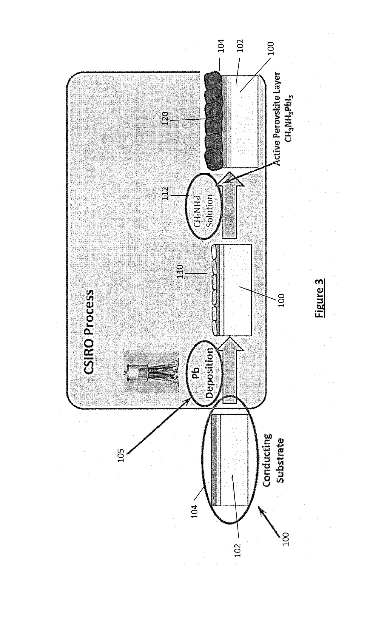
[0263]In this example, a thin metallic Pb seed layer is electrochemically deposited on an n-type compact blocking layer, in this case TiO2, as a precursor for a perovskite solar cell. The deposited Pb seed layer is then chemically converted to the photoactive perovskite material.

[0264]It should be appreciated that whist demonstrated for planar perovskite solar cells, the method and techniques exemplified can equally be applied to non-planar perovskite solar cells configurations for example the inclusion of a mesoscopic thin-film of nanoparticles for example TiO2, Al2O3, ZrO2 or the like.

1.1 Electrochemical Deposition of Pb

[0265]The electrochemical deposition equipment included the following:

[0266]An electrolyte consisting of a 0.01 mol / L solution of Pb(NO3)2 as Pb source and 0.1 mol / L KNO3 as inert conducting electrolyte (also known as supporting electrolyte.

[0267]A working electrode (that where the reacti...

example 2

vaporation of Thin Pb Film as Perovskite Seed Layer for Planar Perovskite Solar Cells

[0275]In the following two examples (2.1 and 2.2), a thin metallic Pb seed layer is formed by thermal evaporation of Pb and condensation onto an n-type compact blocking layer (in this example either ZnO or TiO2) as a precursor for a perovskite solar cell. The seed layer once deposited is then chemically converted to the photoactive perovskite material.

2.1 ZnO Blocking Layer on Indium-Doped Tin Oxide (ITO) Substrate Embodiment

2.1.1 Substrate Preparation

[0276]The ITO substrate was cleaned by successive sonication treatments in detergent (Hellmanex, 1% in milli-W water), pure milli-Q water and isopropanol.

[0277]ZnO blocking layer was applied by spin casting a suspension of ZnO nanoparticles in 1-butanol onto the cleaned ITO substrate. The film was annealed at 100° C. After annealing, the ZnO film was treated by plasma treatment for 1 hour. This was necessary for film stability.

2.1.2 Pb Seed Layer Depos...

example 4 — embodiment

Example 4—Embodiment of Evaporated Pb Seed Layer

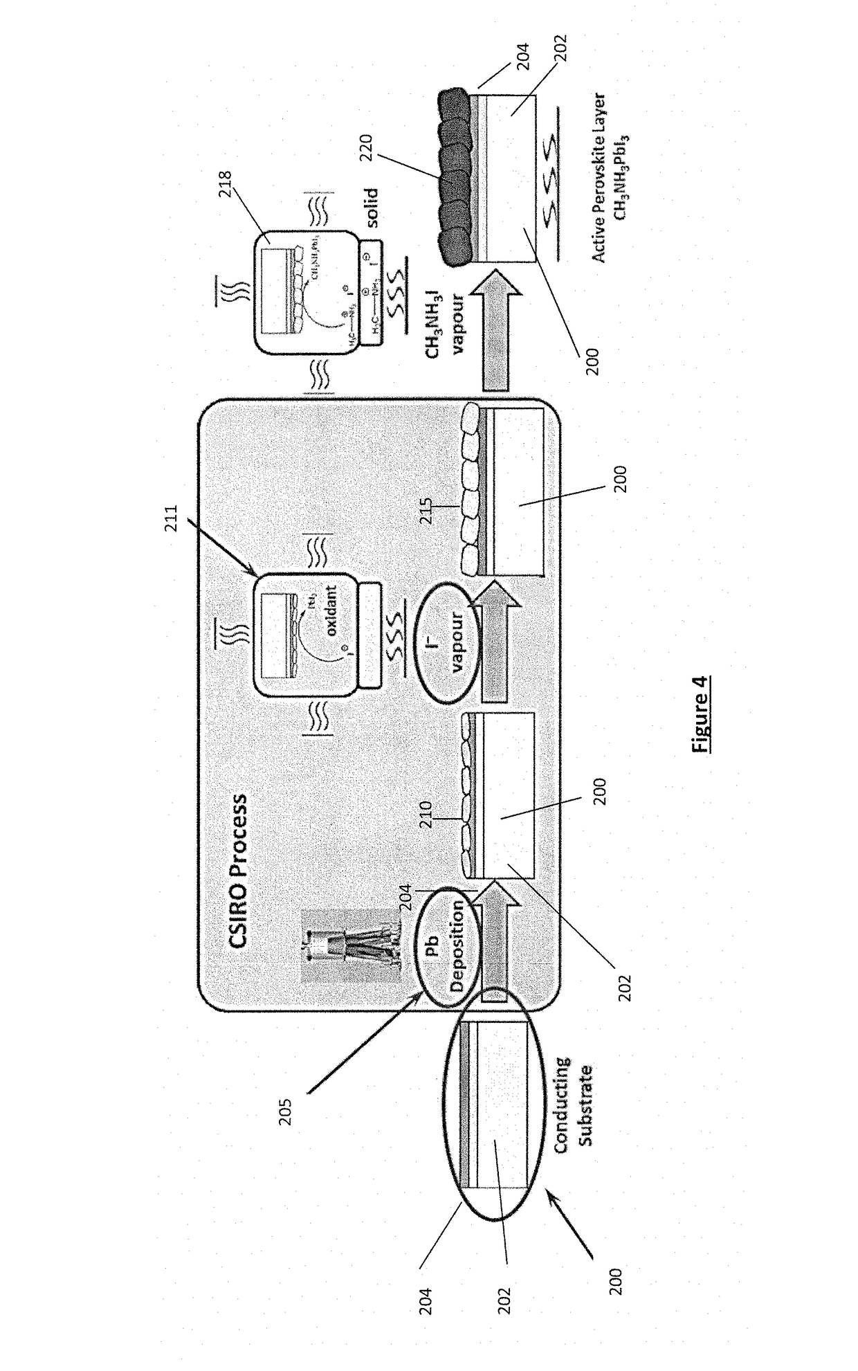
[0294]In the following example, a thin metallic Pb seed layer was formed by thermal evaporation of Pb and condensation onto an n-type compact blocking layer (in this example either ZnO or TiO2) as a precursor for a perovskite solar cell. The seed layer once deposited is then chemically converted using I2 vapour treatment and subsequent exposure to CH3NH3I vapour in a 2-step treatment to form a photoactive perovskite material following the same method outline in Example 2.

[0295]FIG. 13 depicts a calibration plot of evaporated Pb seed thickness against the final perovskite active film thickness as a function of deposited Pb thickness.

[0296]FIG. 14 shows an AFM topography of the layers of a perovskite active film formed from the thermally-evaporated Pb seed layer. This demonstrates that the thin-film maintains the morphology of the FTO substrate from Pb seed layer, to PbI2 and the final CH3NH3PbI3, substantially matching the surface rough...


PUM

PropertyMeasurementUnit
thicknessaaaaaaaaaa
thicknessaaaaaaaaaa
deposition rateaaaaaaaaaa

Abstract

A process of forming a thin film photoactive layer of an optoelectronic device comprising: providing a substrate having a surface comprising or coated with a metal M selected from at least one of Pb, Sn, Ge, Si, Ti, Bi, or In; and converting the metal surface or metal coating of the substrate to a perovskite layer.

Description

TECHNICAL FIELD[0001]The present invention generally relates to a process of forming a photoactive layer of an optoelectronic device. The invention is particularly applicable for perovskite type solar cells and it will be convenient to hereinafter disclose the invention in relation to that exemplary application.BACKGROUND TO THE INVENTION[0002]The following discussion of the background to the invention is intended to facilitate an understanding of the invention. However, it should be appreciated that the discussion is not an acknowledgement or admission that any of the material referred to was published, known or part of the common general knowledge as at the priority date of the application.[0003]Photovoltaic (PV) cells that convert sunlight directly into electricity are becoming increasingly important in the world's renewable energy mix. Currently, around 85% of PV cells have a photoactive element based on crystalline Si, with the rest being polycrystalline thin film PV cells, mos...

Claims


Application Information

Patent Timeline
Patent Type & Authority Patents(United States)
IPC IPC(8): H01L21/00H01L31/0392H01L31/032H01L51/42C25D3/34C25D5/48C25D13/02H01G9/20C23C18/31C25D3/30H01L51/00C25D3/54C23C24/04C23C14/34C23C14/58C23C14/14C23C18/12H01L51/44C23C18/16
CPCH01G9/2059C23C14/34C23C14/5846C23C18/1689C23C18/31C23C24/04C25D3/30C25D3/34C25D3/54C25D5/48C25D13/02H01L31/0324H01L31/0392H01L51/0002H01L51/0032H01L51/4226C23C14/14Y02E10/549C23C18/1216C23C18/1694H01L51/447H10K30/152H10K30/151H10K30/10Y02E10/542H10K85/00H10K30/87H10K85/50H01L31/0216H01L31/0236H01L31/18H10K71/10
Inventor JONES, TIMOTHY WILLIAMWILSON, GREGORY JOSEPHANDERSON, KENRICK FORRESTHOLLENKAMP, ANTHONY FRANKDUFFY, NOEL WILLIAMFIRET, NIENKE JOAN
Owner COMMONWEALTH SCI & IND RES ORG
Why Eureka
Try Eureka