Solar cell module and method for manufacturing the same

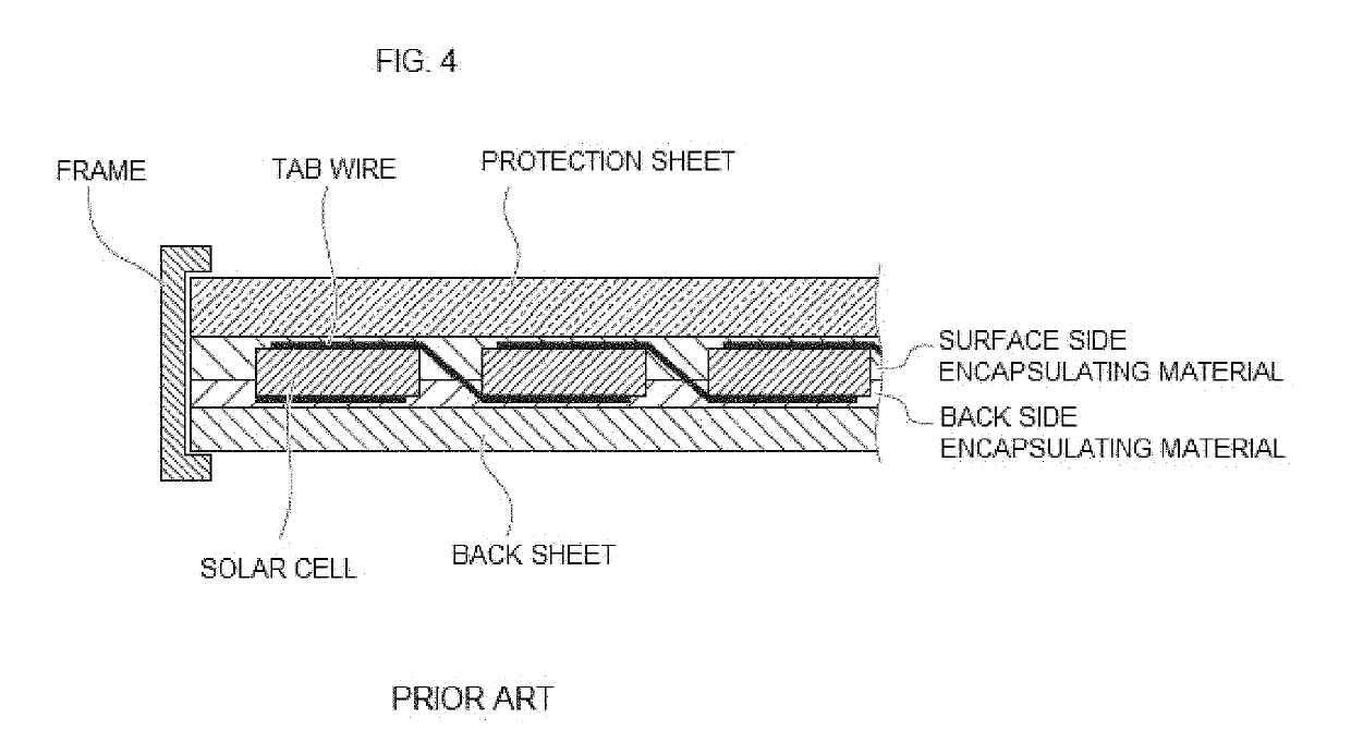
a solar cell and module technology, applied in the field of solar cell modules, can solve the problems of potential difference between the ends of the connected portion, frequent deformation due to potential induced degradation (pid), and high temperature and high humidity in the power generation system, so as to prevent the accumulation of na+ ions, suppress the occurrence of pid damage, and prevent the dissolution and diffusion of na+ ions

Active Publication Date: 2019-07-16
MATERIAL CONCEPT
View PDF24 Cites 0 Cited by
  • Summary
  • Abstract
  • Description
  • Claims
  • Application Information

AI Technical Summary

Benefits of technology

[0046]According to the present invention, it is possible to prevent the dissolution and diffusion of Na+ ions from the protection glass and thus to prevent the accumulation of Na+ ions on the surface of the antireflection film or the transparent conductive film provided on the substrate. Consequently, it is possible to provide a solar cell module which exhibits suppressed occurrence of the PID damage and excellent battery characteristics.

Problems solved by technology

In this MW class power generation system, defects due to potential induced degradation (PID) frequently occur as a problem.
The condition under which the PID damage occurs is that this MW class power generation system is exposed to a high temperature and high humidity environment as well as the potential difference between both ends of the connected portion becomes several hundred volts or more since a large number of panels are connected.
The PID damage is said to be caused because a large potential difference acts between the solar cell and the protection glass and sodium ions (Na+) contained in the protection glass diffuse to the outside from the protection glass due to the potential difference and accumulate on the surface of the antireflection film or the surface of the transparent electrode.
However, the effect of suppressing PID is incomplete as degradation of the solar cell characteristics appears after a PID test has been conducted for 2 hours.

Method used


Image

  • Solar cell module and method for manufacturing the same
  • Solar cell module and method for manufacturing the same
  • Solar cell module and method for manufacturing the same

Examples


example 1

[0086]As a monocrystalline silicon semiconductor substrate, a monocrystalline p-type silicon wafer having a length of 156 mm, a width of 156 mm, and a thickness of 0.2 mm was used. The p-type impurity was boron (B). The upper surface of this wafer was etched with a KOH solution to form a textured framework having an irregular shape. Subsequently, the upper surface of the wafer was coated with POCl3, then phosphorus (P) was diffused into the silicon through heat treatment at a high temperature to form an n+ region, thereby fabricating a monocrystalline silicon semiconductor device having a pn junction.

[0087]Next, a silicon nitride film was formed on the surface of the substrate on the light receiving surface side on which a textured surface was formed at a thickness of 60 nm by plasma enhanced chemical vapor deposition. Thereafter, silver paste and aluminum paste were printed and dried for the formation of the electrode. Thereafter, heat treatment was conducted at 800° C. for 3 secon...

example 2

[0095]A solar cell was fabricated according to the same procedure as in Example 1. Thereafter, a film was formed on the entire surface of the light receiving surface of the solar cell by a sputtering method. By using manganese and silicon sputter targets and controlling the input power to each target, manganese and silicon were deposited on the film while controlling the composition ratio of manganese:silicon=2:1 in atomic % to form a thin alloy film having a thickness of 15 nm. Subsequently, the thin alloy film was subjected to heat treatment at 400° C. for 5 minutes in the air, thereby forming an oxide layer which contained manganese and silicon and had a thickness of 24 nm. The atomic % concentration ratio in the oxide layer was Mn:Si:O=28:14:58.

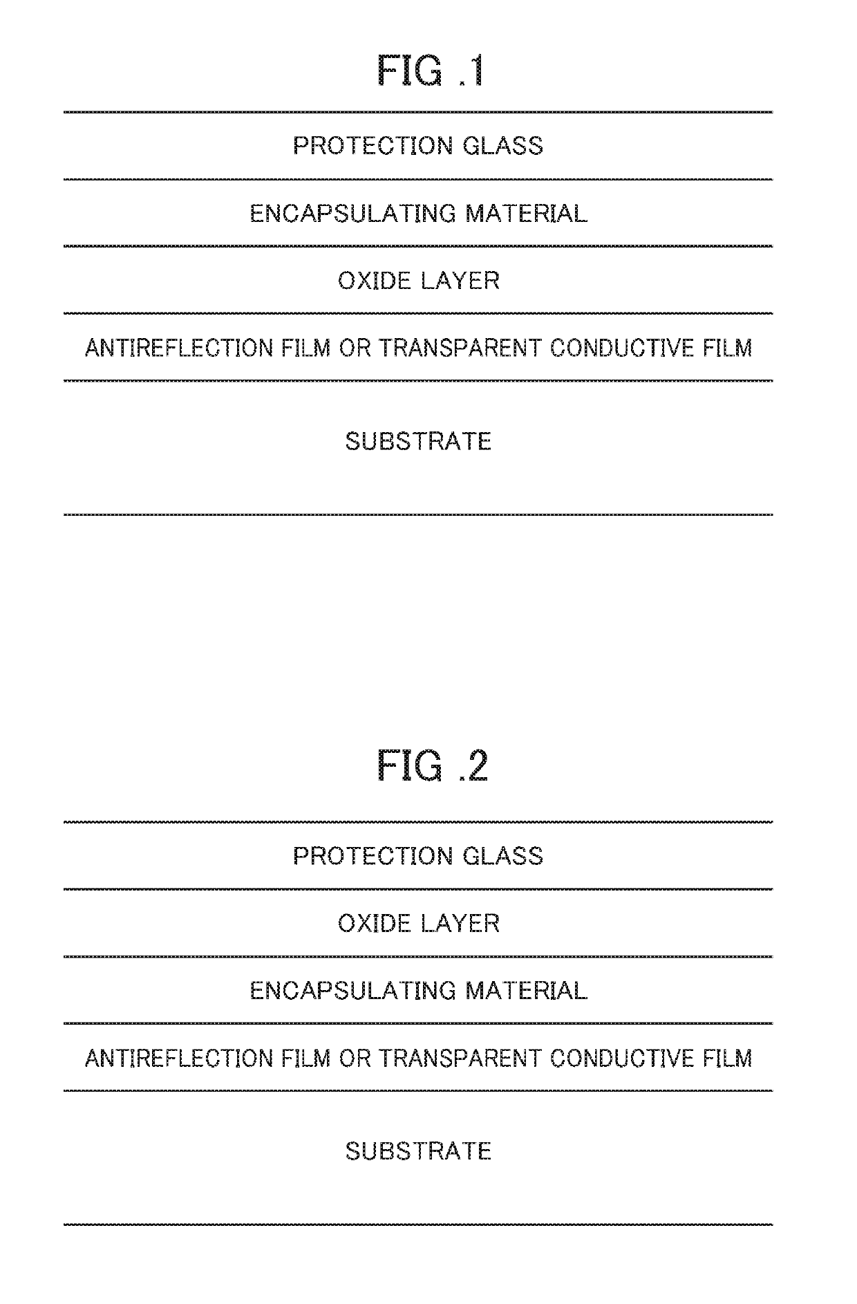
[0096]Next, the surface of the bus electrode of the solar cell was coated with a solder flux and the tab wire was soldered. Thereafter, soda-lime glass, EVA, solar cell, EVA, and back sheet were stacked in this order to form a laminate st...

example 3

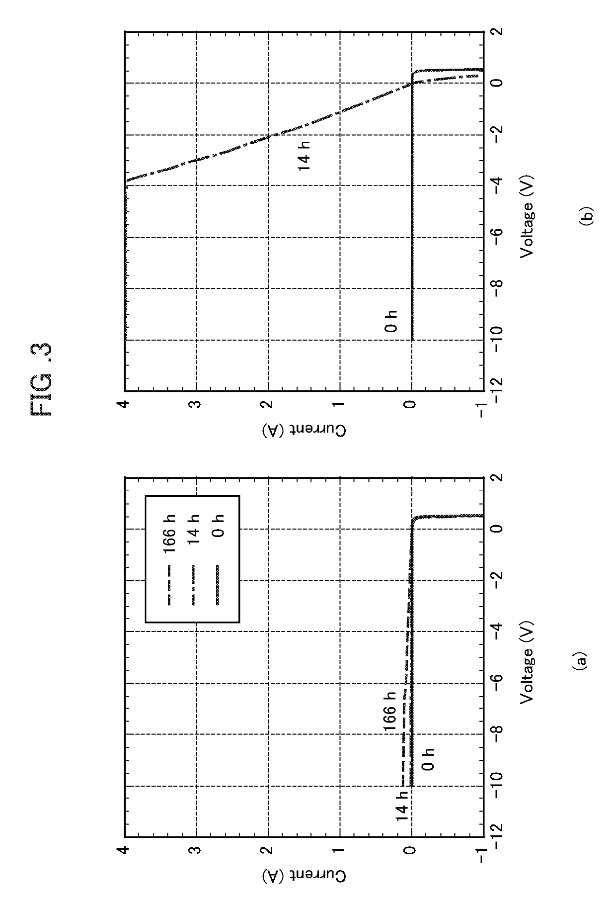
[0098]The influence of the thickness of the oxide layer containing a metal element and silicon was investigated. An oxide layer composed of manganese and silicon was formed by a sputtering method according to the same procedure as in Example 2 except the thickness. By changing the sputtering time, alloy films composed of manganese and silicon with different thicknesses were obtained. Thereafter, the alloy films were subjected to heat treatment to form an oxide layer according to the same procedure as in Example 2 except the thickness, thereby fabricating specimens of solar cell modules having different thicknesses of the oxide layer. These specimens were subjected to the PID test, and the leakage current and conversion efficiency of the solar cell module were measured.

[0099]As the determination criteria, those corresponding to “favorable” (a reference leakage current of 0.5 A or less and a relative decreasing rate of 3% or less) were denoted by “◯”. The results of the test are prese...


PUM


Abstract

A solar cell module capable of preventing the occurrence of a PID failure in a solar photovoltaic power generation system with a MW capacity, said system being used in a high-temperature high-humidity environment; and a method for manufacturing this solar cell module. A solar cell module which comprises a protection glass material and a sealing material on a light receiving surface side of a substrate, and which also comprises an oxide layer between the substrate and the protection glass material, said oxide layer containing a metal element and silicon. It is preferable that the oxide layer contains at least one metal element selected from the group consisting of magnesium, aluminum, titanium, vanadium, chromium, manganese, zirconium, niobium and molybdenum. It is also preferable that the oxide layer has a refractive index of from 1.5 to 2.3 (inclusive) with respect to incident light having a wavelength of 587 nm.

Description

[0001]The present U. S. patent application is a U. S. National Phase Application under 35 U.S.C. 371 of International Application PCT / JP2015 / 085301 filed on Dec. 17, 2015. Priority under 35 U.S.C § 119(a) and 35 U.S.C. § 365(b) is claimed from Japanese Application No. 2014-266406 filed on Dec. 26, 2014, the entirety of which is incorporated herein by references.TECHNICAL FIELD[0002]The present invention relates to a solar cell module that can suppress performance degradation caused by potential induced degradation (PID) and a method of manufacturing the same.BACKGROUND ART[0003]As illustrated in FIG. 4, the solar cell module is composed of a plurality of solar cells and laminating the periphery thereof with a surface protection material (protection glass), an encapsulating material, and a back material (back sheet).[0004]As a manufacturing process of a solar cell, for example, a texture structure is formed on the light receiving surface of a monocrystalline or polycrystalline silico...

Claims


Application Information

Patent Timeline
Patent Type & Authority Patents(United States)
IPC IPC(8): H01L31/18H01L31/0216H01L31/048H01L31/0224
CPCH01L31/02167H01L31/02168H01L31/022466H01L31/0481H01L31/0488H01L31/1876H01L31/048Y02E10/50
Inventor KOIKE, JUNICHISUTOU, YUJIANDO, DAISUKEWADA, MAKOTO
Owner MATERIAL CONCEPT
Why Eureka
Try Eureka