Co-extruded one-time-formed solar cell module backboard in three-layer structure
a solar cell module and backboard technology, applied in the field of one-time-formed solar cell module backboard in a three-layer structure, can solve the problems of poor heat conduction efficiency and heat resistance, low rate, and affect the power generation efficiency of the cell, and achieve good long-term ageing resistance, high water resistance ratio, and high reflective rate
- Summary
- Abstract
- Description
- Claims
- Application Information
AI Technical Summary
Benefits of technology
Problems solved by technology
Method used
Image
Examples
embodiment 1
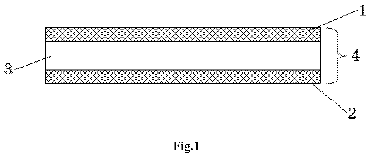
[0030]FIG. 1 is a structural schematic diagram of a solar cell module backboard (4) in a three-layer structure. The solar cell module backboard (4) comprises a middle layer (3) which is located in the middle as well as an outer layer (1) and an outer layer 2 which are located at the two sides of the middle layer, and is made by three-layer co-extrusion one-time continuous production, namely, hybrid polymerized films are formed by a high-temperature co-extrusion film making process,
[0031]wherein the outer layer (1) comprises raw materials (by mass percent, similarly hereinafter) of 88% of PA12 and 12% of TiO2 and is 0.050 mm in thickness;
[0032]the chemical formula of the outer layer (1) is: [NH—(CH2)11—CO]n; the inner layer (2) comprises raw materials of 19% of EVA, 69% of LLDPE and 12% of TiO2 and is 0.050 mm in thickness;
[0033]the chemical formula of the inner layer (2) is: (C2H4)×(C4H)2)+(C2H4)n,
[0034]wherein the chemical formula of EVA is: (C2H4)×(C4H6O2)y, and the chemical formu...
embodiment 2
[0038]FIG. 1 is a structural schematic diagram of a solar cell module backboard (4) in a three-layer structure. The solar cell module backboard (4) comprises a middle layer (3) which is located in the middle as well as an outer layer (1) and an outer layer 2 which are located at the two sides of the middle layer,
[0039]wherein the outer layer (1) comprises raw materials of 88% of PA12 and 12% of TiO2 and is 0.050 mm in thickness;
[0040]the chemical formula of PA12 is: [NH—(CH2)11—CO]n;
[0041]the inner layer (2) comprises raw materials of 88% of PA12 and 12% of TiO2 and is 0.050 mm in thickness;
[0042]the middle layer (3) comprises raw materials of 98% of PA12 and 2% of TiO2 and is 0.250 mm in thickness;
[0043]Hybrid polymerized films are formed by a high-temperature co-extrusion film making process.
embodiment 3
[0044]FIG. 1 is a structural schematic diagram of a solar cell module backboard (4) in a three-layer structure. The solar cell module backboard (4) comprises a middle layer (3) which is located in the middle as well as an outer layer (1) and an outer layer 2 which are located at the two sides of the middle layer, and is made by three-layer co-extrusion one-time continuous production,
[0045]wherein the outer layer (1) comprises raw materials of 65% of HDPE-g-GMA, 23% of PA12 and 12% of TiO2 and is 0.050 mm in thickness, and the chemical formula of HDPE is: [—CH2—CH2-]n;
[0046]the inner layer (2) comprises raw materials of 65% of HDPE-g-GMA, 23% of PA112 and 12% of TiO2 and is 0.050 mm in thickness; and
[0047]the middle layer (3) comprises raw materials of 58% of HOPP, 20% of PP-g-GMA, 20% of PA12 and 2% of TiO2 and is 0.250 mm in thickness. A crosslinking reaction is carried out on a part of raw materials by a high-temperature co-extrusion film making process, so as to form hybrid polym...
PUM
| Property | Measurement | Unit |
|---|---|---|
| thickness | aaaaa | aaaaa |
| thickness | aaaaa | aaaaa |
| thickness | aaaaa | aaaaa |
Abstract
Description
Claims
Application Information


