Deposition of a coating on an interconnect for solid oxide cell stacks
- Summary
- Abstract
- Description
- Claims
- Application Information
AI Technical Summary
Benefits of technology
Problems solved by technology
Method used
Image
Examples
example 1
[0045]Co Deposition by Electroplating
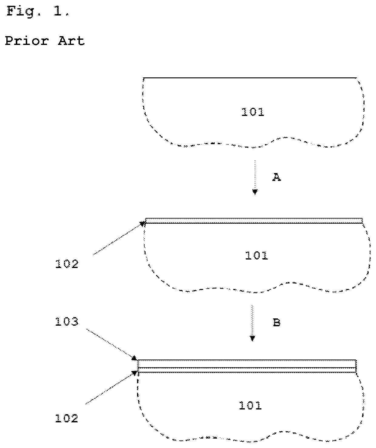
[0046]FIG. 1 presents a schematic process diagram of the method for the electrodeposition of cobalt that can be considered prior art. An interconnect substrate comprising Cr and Fe 101 is first covered with a strike layer of nickel or cobalt 102. This step is explained as A in FIG. 1. The electrodeposition of the first metallic layer can be done for example by using the Woods process. Other formulations such as the sulfamate strike can also be used for this purpose. The current densities used in the deposition of the first layer should be in the range of 1-10 A / dm2. The second metallic layer of Co 103 is electrodeposited from a Watts type or another acidic electrolyte (such as chloride, sulfate, sulfamate, ammonium sulfate, fluoroborate and mixtures thereof) with a current density ranging from 0.5 to 5 A / dm2. This step is explained as B in FIG. 1. The thickness of the second metallic Co layer 103 is between 0.5 μm and 10 μm, preferably between 1 ...
example 2
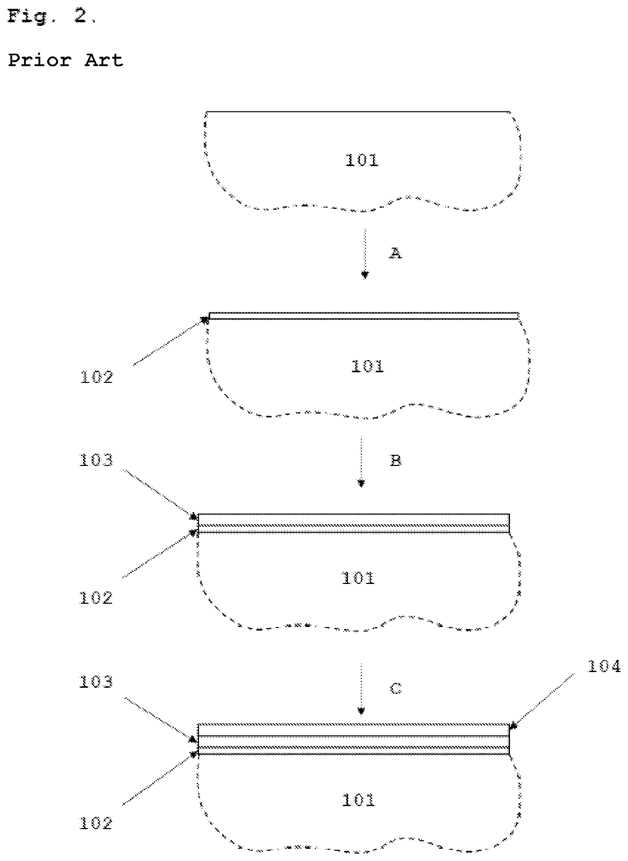
[0047]Co—Cu deposition by electroplating from alkaline solutions FIG. 2 presents a schematic process diagram of the method for the electrodeposition of cobalt and copper that can be considered prior art. The deposition proceeds according to the method described in Example 1, except that after the electrodeposition of the second metallic Co layer 103, a layer of metallic Cu 104 is deposited by electrodeposition from an alkaline cyanide-based electrolyte solution. This step is explained as C in FIG. 2. The current densities used in the deposition of the Cu layer 104 range from 1 to 6 A / dm2. The growth of the Cu layer from alkaline cyanide-based electrolyte solutions thus requires external electric field to be applied to the galvanic cell and is not self-limiting in nature.
example 3
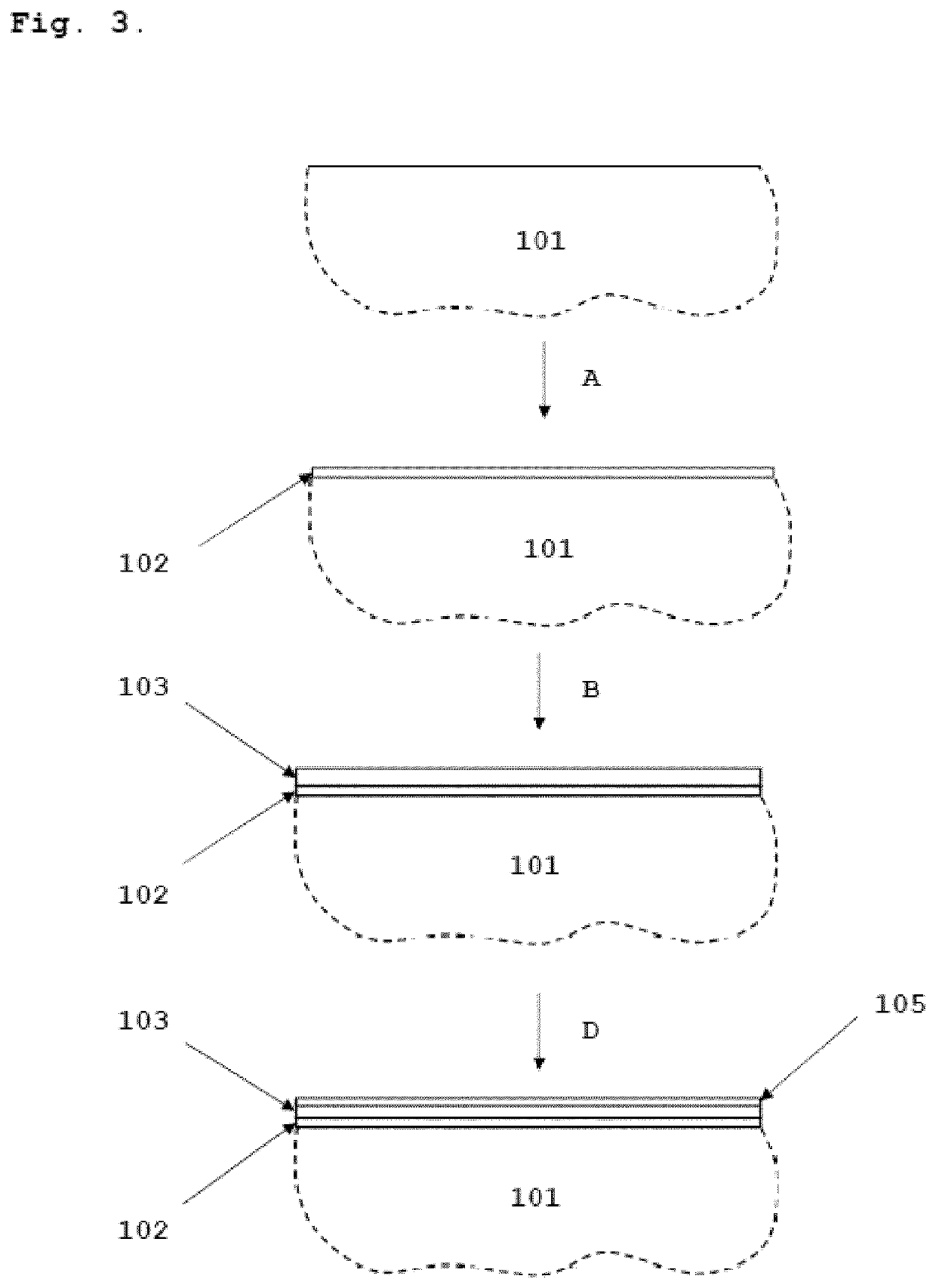
[0048]FIG. 3 presents a schematic process diagram of the present invention for electrodeposition of cobalt and ion-exchange plating of copper. An interconnect substrate comprising Cr and Fe 101 is first covered with a strike layer of nickel or cobalt 102. This step is explained as A in FIG. 3. The electrodeposition of the first metallic layer can be done for example by using the Woods process or a sulfamate strike. The current densities used in the deposition of the first layer should be in the range of 1-10 A / dm2. The second metallic layer of Co 103 is electrodeposited from an acidic electrolyte (such as chloride, sulfate, sulfamate, ammonium sulfate, fluoroborate and mixtures thereof) with a current density ranging from 0.5 to 5 A / dm2. This step is explained as B in FIG. 3. The thickness of the second metallic Co layer 103 is between 0.5 μm and 10 μm, preferably between 1 μm and 6 μm. A third metallic layer of Cu 105 is then deposited onto resulting structure by ion-exchange plati...
PUM
| Property | Measurement | Unit |
|---|---|---|
| Thickness | aaaaa | aaaaa |
| Thickness | aaaaa | aaaaa |
| Thickness | aaaaa | aaaaa |
Abstract
Description
Claims
Application Information


