Semiconductor device including a reactant metal layer disposed between an aluminum alloy film and a catalyst metal film and method for manufacturing thereof

a technology of reactant metal layer and catalyst metal layer, which is applied in the direction of liquid/solution decomposition chemical coating, vacuum evaporation coating, coating, etc., can solve the problems of high manufacturing cost, increased warping of semiconductor wafers, and difficult patterning, so as to reduce contamination of semiconductor substrates

Active Publication Date: 2021-03-02
MITSUBISHI ELECTRIC CORP
View PDF7 Cites 0 Cited by
  • Summary
  • Abstract
  • Description
  • Claims
  • Application Information

AI Technical Summary

Benefits of technology

[0011]According to the present invention, a reactant layer is disposed between an aluminum alloy film and a catalyst metal film and contains metal of the catalyst metal film. Accordingly, the reactant layer reduces contamination of a semiconductor substrate with, for example, a degreasing solution, an electroless Ni plating solution, and an electroless Au plating solution in plating treatment.

Problems solved by technology

Manufacturing cost is high and patterning is difficult when such a relatively thick Ni film is formed by evaporation coating or sputtering deposition.
However, the warping of the semiconductor device, that is, the warping of the semiconductor wafer increases with the thinning of the semiconductor device and the thickening of the Ni film as a front-surface electrode.
As a result, handling of the semiconductor device becomes difficult, and solder is likely to contain voids at mounting on a circuit board and the voids cause bonding defects, which has resulted in decrease of the yield.
However, the above-described zincate treatment has such a problem that the Al alloy electrode is locally anomalously etched by chemical solution of degreasing, pickling, and zincate treatment, and disappears.
This disappearance occurs due to anomaly of the film quality of the Al alloy electrode and foreign matter in the film.
When the Al alloy electrode disappears in this manner, the underlaying semiconductor substrate is contaminated through exposure to the chemical solution, and the electric property thereof degrades.

Method used


Image

  • Semiconductor device including a reactant metal layer disposed between an aluminum alloy film and a catalyst metal film and method for manufacturing thereof
  • Semiconductor device including a reactant metal layer disposed between an aluminum alloy film and a catalyst metal film and method for manufacturing thereof
  • Semiconductor device including a reactant metal layer disposed between an aluminum alloy film and a catalyst metal film and method for manufacturing thereof

Examples


first embodiment

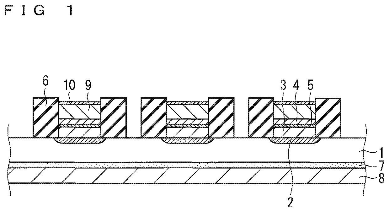
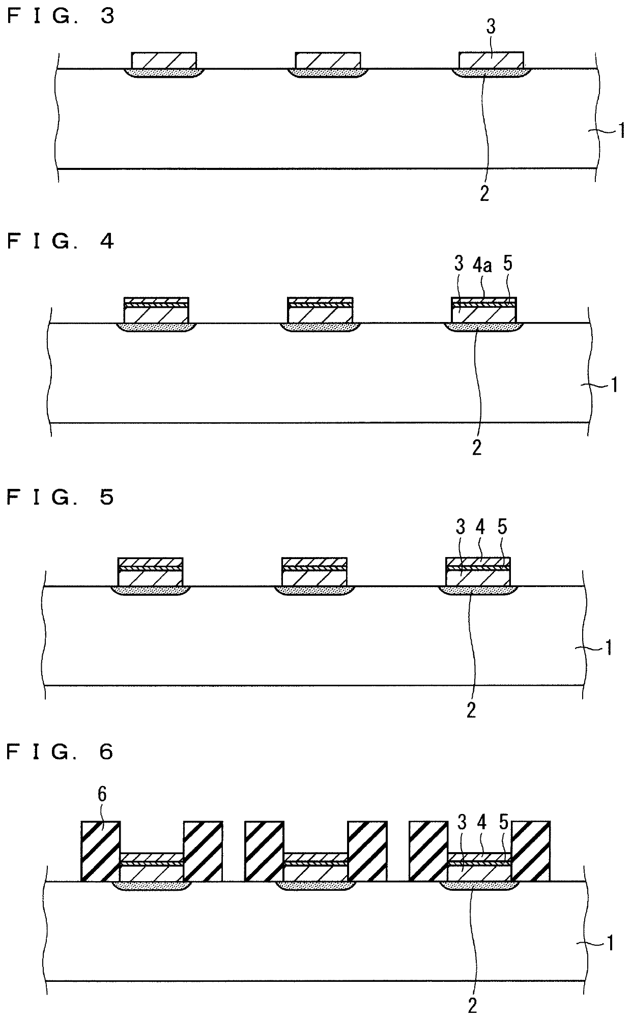
[0038]FIG. 1 is a cross-sectional view illustrating a configuration of a semiconductor device according to a first embodiment of the present invention. The semiconductor device illustrated in FIG. 1 includes a semiconductor wafer 1, a front-surface semiconductor element region 2, a front-surface Al alloy film 3, a front-surface Au film 4, a front-surface reactant layer 5, a polyimide protective film 6, a back-surface diffusion region 7, a back-surface electrode 8, a front-surface electroless Ni plating film 9, and a front-surface electroless Au plating film 10 as an electroless gold plating film. The front-surface Al alloy film 3, the front-surface Au film 4, the front-surface reactant layer 5, the front-surface electroless Ni plating film 9, and the front-surface electroless Au plating film 10 are used as electrodes on the front side of the semiconductor wafer 1.

[0039]The semiconductor wafer 1 as a semiconductor substrate is made of, for example, silicon (Si) or a wide-bandgap semi...

second embodiment

[0063]FIG. 11 is a cross-sectional view illustrating a configuration of a semiconductor device according to the second embodiment of the present invention. Hereinafter, among components described in the second embodiment, a component same as or similar to that in the first embodiment is denoted by the same reference sign, and any different component will be mainly described.

[0064]The semiconductor device illustrated in FIG. 11 includes the semiconductor wafer 1, the front-surface semiconductor element region 2, the front-surface Al alloy film 3, the polyimide protective film 6, the back-surface diffusion region 7, a back-surface Al alloy film 11, a back-surface Au film 12, a back-surface reactant layer 13, a back-surface electroless Ni plating film 14, and a back-surface electroless Au plating film 15.

[0065]In the second embodiment, the back-surface Al alloy film 11, the back-surface Au film 12, the back-surface reactant layer 13, the back-surface electroless Ni plating film 14, and...

third embodiment

[0078]FIG. 19 is a cross-sectional view illustrating a configuration of a semiconductor device according to a third embodiment of the present invention. Hereinafter, among components described in the third embodiment, a component same as or similar to those in Embodiments 1 and 2 is denoted by the same reference sign, and any different component will be mainly described.

[0079]The semiconductor device illustrated in FIG. 19 includes the semiconductor wafer 1, the front-surface semiconductor element region 2, the front-surface Al alloy film 3, the front-surface Au film 4, the front-surface reactant layer 5, the polyimide protective film 6, the back-surface diffusion region 7, the front-surface electroless Ni plating film 9, the front-surface electroless Au plating film 10, the back-surface Al alloy film 11, the back-surface Au film 12, the back-surface reactant layer 13, the back-surface electroless Ni plating film 14, and the back-surface electroless Au plating film 15.

[0080]In the t...


PUM

PropertyMeasurementUnit
thicknessaaaaaaaaaa
thicknessaaaaaaaaaa
thicknessaaaaaaaaaa

Abstract

A technology capable of reducing contamination of a semiconductor substrate above which a nickel film is disposed is provided. A semiconductor device includes: a semiconductor substrate; an aluminum alloy film disposed on at least one of a front surface and a back surface of the semiconductor substrate; a catalyst metal film disposed above the aluminum alloy film and exhibiting catalytic activity for autocatalytic reaction that deposits nickel; an electroless nickel plating film disposed on the catalyst metal film; and a reactant layer disposed between the aluminum alloy film and the catalyst metal film and containing metal of the catalyst metal film.

Description

TECHNICAL FIELD[0001]The present invention relates to a semiconductor device including a nickel film, and a method for manufacturing the same.BACKGROUND ART[0002]In the process of manufacturing a vertically conductive semiconductor device such as an insulated gate bipolar transistor (IGBT) or a diode, a semiconductor wafer is fabricated to be thin to reduce resistance at conduction and improve the current-voltage characteristic. Some recent semiconductor wafers are thinned to have a thickness of 50 μm approximately.[0003]In the mainstream conventional technology of mounting such a vertically conductive semiconductor device onto a circuit board, solder bonding is performed on a back-surface electrode of the semiconductor device to achieve wire bonding for connecting, for example, an aluminum wire to the front-surface electrode. However, recently, the technology of solder bonding on both surfaces of a front-surface electrode and a back-surface electrode of the semiconductor device has...

Claims


Application Information

Patent Timeline
Patent Type & Authority Patents(United States)
IPC IPC(8): H01L21/288H01L23/532H01L21/28C23C18/18C23C18/32C23C18/42H01L21/02
CPCH01L21/288C23C18/1879C23C18/32C23C18/42H01L21/02068H01L21/28H01L23/53219H01L23/53223H01L24/00H01L21/76874H01L24/03H01L24/05H01L2224/06181H01L2224/0401H01L2224/04026H01L2224/05084H01L2224/0348H01L2224/03464H01L2224/0345H01L2224/0381H01L2224/02126C23C18/34C23C18/18C23C14/025C23C14/165C23C14/5806H01L2224/05144H01L2224/05166H01L2224/05157H01L2224/05138H01L2224/05644H01L2224/05147H01L2224/05124H01L2224/05155H01L2224/05164H01L2924/00012H01L2924/013H01L2924/01014H01L2924/01029H01L2924/00014H01L2924/01013H01L2924/01079
Inventor UENO, RYUJISUNAMOTO, MASATOSHI
Owner MITSUBISHI ELECTRIC CORP
Why Eureka
Try Eureka