

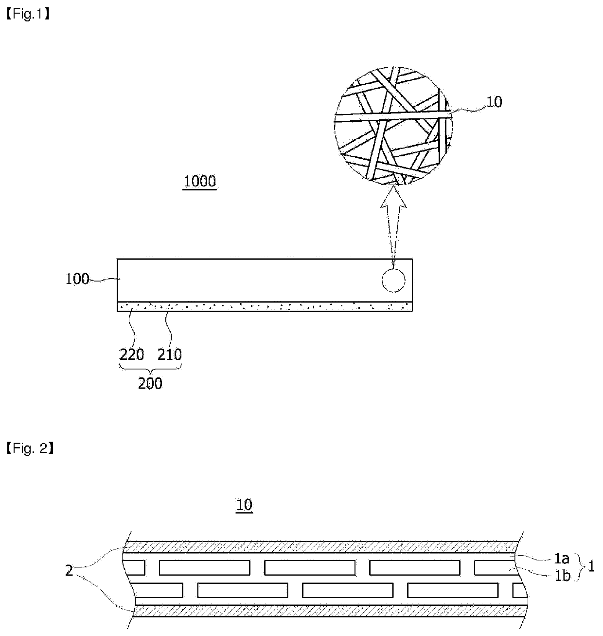
Flexible electromagnetic wave shielding material, electromagnetic wave shielding type circuit module comprising same and electronic device furnished with same
a technology of electromagnetic shielding and electromagnetic wave shielding, which is applied in the direction of shielding materials, printed circuit non-printed electric components association, electrical apparatus contruction details, etc., can solve the problems of malfunction of electronic devices, user who is using electronic devices may be harmfully affected, and cannot be easily shielded, so as to prevent deterioration of electromagnetic wave shielding performance, excellent flexibility, and creasing/recovery
- Summary
- Abstract
- Description
- Claims
- Application Information
AI Technical Summary
Benefits of technology
Problems solved by technology
Method used
Image

Examples
embodiment 1
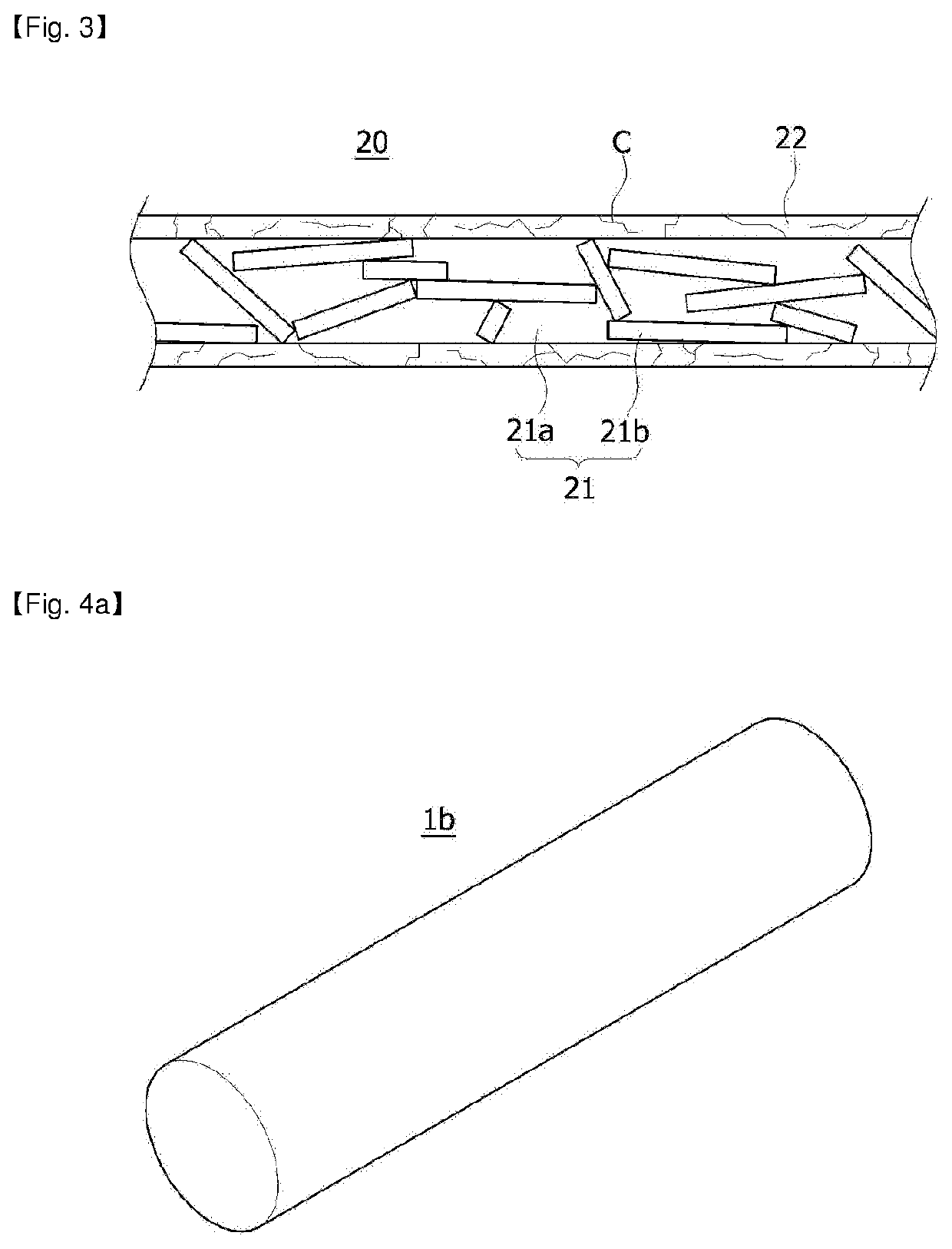
[0217]A spinning solution was manufactured by dissolving 12 g of polyvinylidene fluoride in 88 g of dimethylacetamide and acetone, which were mixed at a weight ratio of 70:30, using a magnetic bar at a temperature of 80° C. for 6 hours. Spherical silver particles having an average particle diameter of 1.3 μm were mixed with the spinning solution as conductive fillers such that the polyvinylidene fluoride and the sliver particles had a volume ratio of 1:0.2 and the sliver particles occupied 16.7% of the total volume of the final fiber part, and then were dispersed using an ultrasonic disperser for 12 hours. The spinning solution was poured into a solution tank of an electrospinning apparatus, stirred through an impeller, and then discharged at a rate of 20 μL / min / hole. In this case, a fiber web formed of an Ag / PVDF composite fiber in which a second part with no silver particles had an average diameter of 300 nm was manufactured by maintaining the temperature and humidity of the spinn...
embodiments 2 to 11
[0219]A conductive fiber web as shown in Table 1 was manufactured in the same way as in Embodiment 1, except that the amount and particle diameter of the conductive fillers were changed as shown in Table 1 or Table 2 below.
experimental example 1
[0221]The following physical properties of the conductive fiber webs according to Embodiments 1 to 11 and Comparative Example 1 were measured and shown in Table 1 and Table 2 below.
[0222]1. Initial Electromagnetic Wave Shielding Performance
[0223]The surface resistance of the conductive fiber web was measured through a resistance meter (HIOKI 3540 mΩ HITESTER, HIOKI). The measured resistance value according to the embodiment was expressed by a relative percentage with respect to the measured resistance value of Comparative Example 1 being set to 100.
[0224]2. Electromagnetic Wave Shielding Performance Variation
[0225]A specimen was elongated by a factor of 1.2 in the transverse direction and then by a factor of 1.2 in the longitudinal direction by means of a jig. This process was repeated three times.
[0226]Subsequently, a resistance value B for each specimen after elongation was found using the method of measuring the initial electromagnetic wave shielding performance, and a variation ...
PUM
| Property | Measurement | Unit |
|---|---|---|
| diameter | aaaaa | aaaaa |
| thickness | aaaaa | aaaaa |
| thickness | aaaaa | aaaaa |
Abstract
Description
Claims
Application Information