Reflective mask blank and reflective mask

a mask and reflective technology, applied in the field of reflective masks and mask blanks, can solve the problems of dielectric breakdown, the limit of a conventional photolithography method has been approached, and the semiconductor device processing is accelerating, so as to avoid the deformation of the substrate caused by stress, improve the position deviation of a pattern during transfer, and ensure the effect of a sufficient holding for

Active Publication Date: 2021-06-15
ASAHI GLASS CO LTD
View PDF21 Cites 0 Cited by
  • Summary
  • Abstract
  • Description
  • Claims
  • Application Information

AI Technical Summary

Benefits of technology

[0015]In order to solve the above-mentioned problems of conventional techniques, an object of the present invention is to provide a reflective mask blank including a backside conductive layer and a mask blank, which have the following properties: light transmittance over the wavelength range of 400 nm to 800 nm is high; a sheet resistance value is low; and deformation of a substrate can be corrected by adjusting internal stress.
[0033]In the reflective mask blank, since the light transmittance of the backside conductive film over the wavelength range of 400 nm to 800 nm is 10% or more, positional deviation of a pattern during transfer can be improved by locally irradiating a back surface of the EUV mask which is obtained by forming a pattern in the absorber layer with a pulsed laser in the wavelength region, so as to locally heat the glass substrate.
[0035]Further, the backside conductive film is a film having a compressive stress with a total stress of 50 Pa·m to 400 Pa·m, so that stress generated on a front surface side (a reflective layer side) of the substrate and stress generated on a back surface side of the substrate are canceled with each other, and as a result, deformation of the substrate caused by application of stress can be avoided.

Problems solved by technology

However, fining of semiconductor devices is accelerating, but a limit of a conventional photolithography method has been approached.
Therefore, in a case of a substrate having a low dielectric constant and low conductivity such as a glass substrate, in order to obtain the same degree of chucking force as in a Si wafer, it is necessary to apply high voltage, which may cause a risk of dielectric breakdown.
Generally, in order to increase the light transmittance, a thickness may be reduced, but when the thickness of the backside conductive film is thin, a sheet resistance value thereof may increase and these requirements may not be satisfied.
Further, in the EUV mask and the reflective mask blank used therein, there may be a problem of substrate deformation caused by internal stress in the multilayer reflective film as the reflective layer, or the absorber layer.

Method used


Image

  • Reflective mask blank and reflective mask

Examples


case 1

(Case 1)

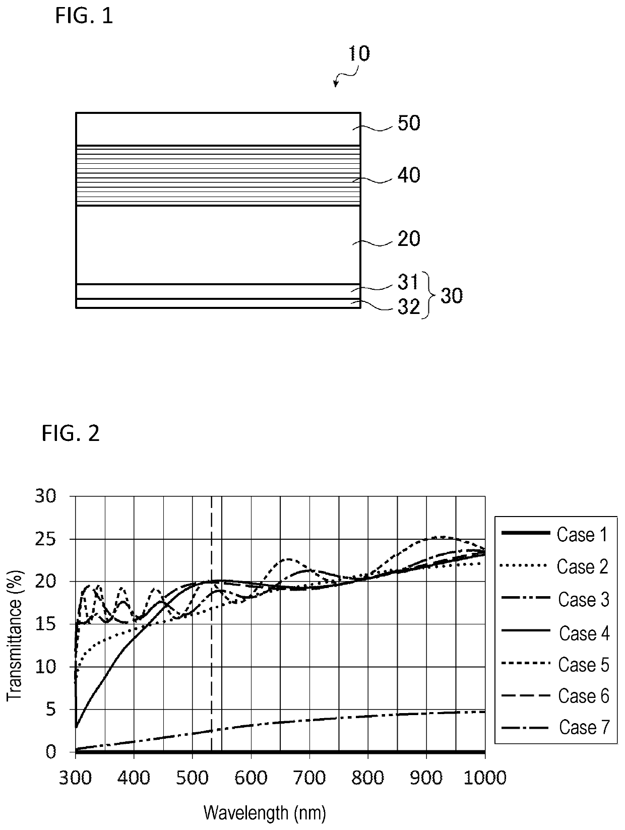
[0128]In this Case 1, the conductive layer 32 was formed without forming the stress compensation layer 31 on one surface side of the substrate 20.

[0129]A SiO2—TiO2 based glass substrate (6 inches (about 152 mm) square in outer dimensions, and 6.3 mm thick) was used as the substrate 20 for the deposition. The glass substrate has a coefficient of thermal expansion of 0.05×10⁻⁷ / ° C. at 20° C., a Young's modulus of 67 GPa, a Poisson's ratio of 0.17, and a specific rigidity of 3.07×10⁷ m2 / s2. The glass substrate is polished to form a smooth surface with a surface roughness (rms) of 0.15 nm or less and flatness of 100 nm or less.

[0130]A CrN film was formed as a conductive layer 32 on one surface side of the substrate 20 by use of a magnetron sputtering method. The deposition conditions for the conductive layer 32 (CrN film) are as follows.

[0131]Target: Cr target

[0132]Sputtering Gas: mixed gas of Ar and N2 (gas flow (Ar / N2): 21 / 20 (sccm), gas pressure: 0.23 Pa)

[0133]Input Power: 1,...

case 2

(Case 2)

[0163]A CrO film was formed as the stress compensation layer 31 on one surface side of the substrate 20 by use of a magnetron sputtering method. The deposition conditions for the stress compensation layer 31 (CrO film) are as follows.

[0164]Target: Cr target

[0165]Sputtering Gas: mixed gas of Ar and O2 (gas flow (Ar / O2): 35 / 20 (sccm), gas pressure: 0.3 Pa)

[0166]Input Power: 700 W

[0167]Deposition Rate: 0.101 nm / sec

[0168]Film Thickness: 14 nm

[0169]Next, a CrN film was formed as the conductive layer 32 on the stress compensation layer 31 by use of the magnetron sputtering method, thereby forming the backside conductive film 30. The deposition conditions for the conductive layer 32 (CrN film) are as follows.

[0170]Target: Cr target

[0171]Sputtering Gas: mixed gas of Ar and N2 (gas flow (Ar / N2): 30 / 10 (sccm), gas pressure: 0.23 Pa)

[0172]Input Power: 700 W

[0173]Deposition Rate: 0.065 nm / sec

[0174]Film Thickness: 14 nm

[0175]The stress compensation layer 31 and the backside conductive fi...

case 3

(Case 3)

[0177]The backside conductive film 30 was formed by performing the same procedures as in the Case 2 except that the thickness of the stress compensation layer 31 (CrO film) was 30 nm and the thickness of the conductive layer 32 (CrN film) was 40 nm.

[0178]The stress compensation layer 31 and the backside conductive film 30 in the Case 3 were evaluated in the same procedures as in the Case 1, and the results were shown in Table 1 and Table 2.

[0179]As a result of the flatness of the reflective mask blank obtained in the same procedures as in the Case 1, the flatness was 1,110 nm and the reflective mask blank had a convex shape on the side where the reflective layer was formed.


PUM

PropertyMeasurementUnit
thicknessaaaaaaaaaa
thicknessaaaaaaaaaa
thicknessaaaaaaaaaa

Abstract

A reflective mask blank includes a backside conductive film on a back surface of a substrate. The backside conductive film has a laminated structure including a stress compensation layer and a conductive layer in this order from the substrate side. The conductive layer includes a metal nitride. The stress compensation layer has a compressive stress and the stress compensation layer includes at least one compound selected from the group consisting of oxides, oxynitrides, and nitrides, each having an absorption coefficient (k) over the wavelength range of 400 nm to 800 nm being 0.1 or less. The conductive layer has a thickness of 5 nm or more and 30 nm or less. The backside conductive film has a total thickness of 50 nm or more.

Description

BACKGROUND OF THE INVENTIONTechnical Field[0001]The present invention relates to a reflective mask blank to be used in EUV (Extreme Ultra Violet) lithography used in semiconductor manufacturing or the like, and a reflective mask obtained by forming a pattern in an absorber layer of the reflective mask blank.Background Art[0002]In semiconductor industry, a photolithography method using visible light or ultraviolet light has been used as a fine pattern transfer technique necessary for forming an integrated circuit including a fine pattern on a Si substrate or the like. However, fining of semiconductor devices is accelerating, but a limit of a conventional photolithography method has been approached. In the photolithography method with single exposure, a resolution limit of a pattern is about ½ of an exposure wavelength, and it has been said that the resolution limit of the pattern is about ¼ of the exposure wavelength even when an immersion method is used, and the limit is expected to...

Claims


Application Information

Patent Timeline
Patent Type & Authority Patents(United States)
IPC IPC(8): G03F1/24G03F1/38G03F1/40G03F1/48G03F1/52G03F1/54
CPCG03F1/40G03F1/24G03F1/38G03F1/48G03F1/52G03F1/54
Inventor KAWAHARA, HIROTOMOHANEKAWA, HIROSHIUNO, TOSHIYUKI
Owner ASAHI GLASS CO LTD
Why Eureka
Try Eureka