Low temperature thin film transistor fabrication

a thin film transistor and fabrication technology, applied in transistors, thermoelectric devices, solid-state devices, etc., can solve the problems of not being able to withstand temperatures above 150-200 degrees c and meeting all constraints, and achieve the effect of broadening the range of materials and processes availabl

Inactive Publication Date: 2001-08-23
GLOBALFOUNDRIES INC
View PDF0 Cites 51 Cited by
  • Summary
  • Abstract
  • Description
  • Claims
  • Application Information

AI Technical Summary

Benefits of technology

0006] The invention broadens the range of materials and processes available for TFT devices by providing in the device structure an organic semiconductor layer that is in contact with an inorganic mixed oxide gate insulator involving processing with the types of processing techniques that can take place in a temperature range from about room temperature to about 150 degrees C.

Problems solved by technology

Meeting all the constraints is becoming more difficult to achieve.
Transparent plastic substrates for AMLCD are very desirable but cannot withstand temperatures above 150-200 degrees C.

Method used


Image

  • Low temperature thin film transistor fabrication
  • Low temperature thin film transistor fabrication
  • Low temperature thin film transistor fabrication

Examples


example 1

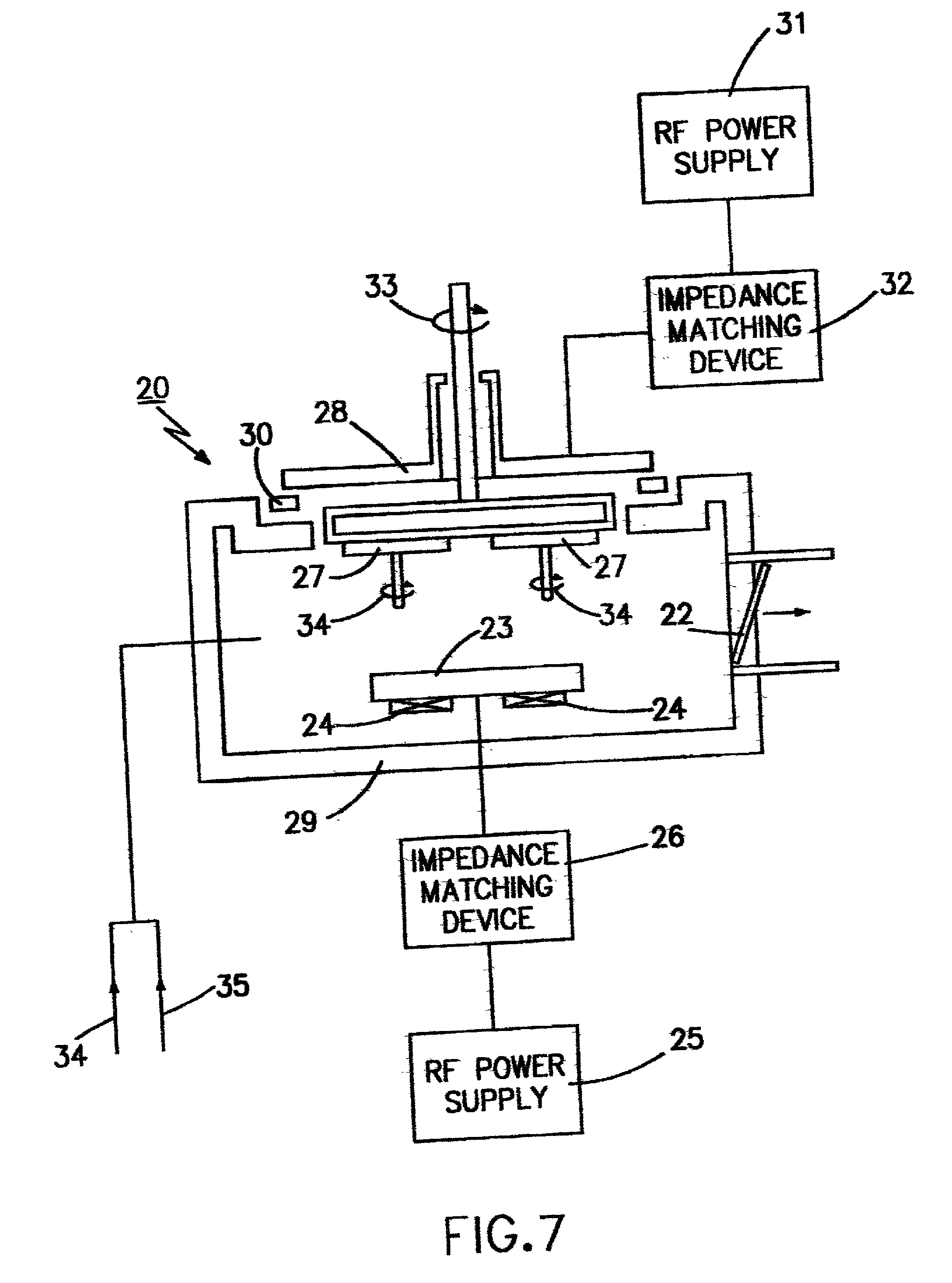
[0041] Substrates such as silicon wafers with a blanket coating of 150 .ANG. titanium followed by 400 .ANG. of platinum can be loaded into a BZT sputter deposition chamber as described in connection with FIG. 7. The chamber is pumped down to a base pressure of 2.1.times.10.sup.-7 torr after which a flow of 10 standard cubic centemeters per minute (sccm) of argon and 2 sccm of oxygen gas are introduced into the chamber through elements 34 and 35. By appropriate valving of the chamber, a total pressure of 2 mtorr is achieved. After purging this gas for 5 minutes, a plasma is ignited in the chamber by applying a radio frequency ac voltage through elements 25 and 26 to the BZT sputter target 23 while maintaining the chamber at ground potential. The ions in the rf plasma thus created is used to reactively sputter the BZT from the target on to the samples 27 loaded in the chamber. A total power of 100 watts which corresponds to a power density of about 0.8 watts / cm.sup.2 is employed to ac...

example 2

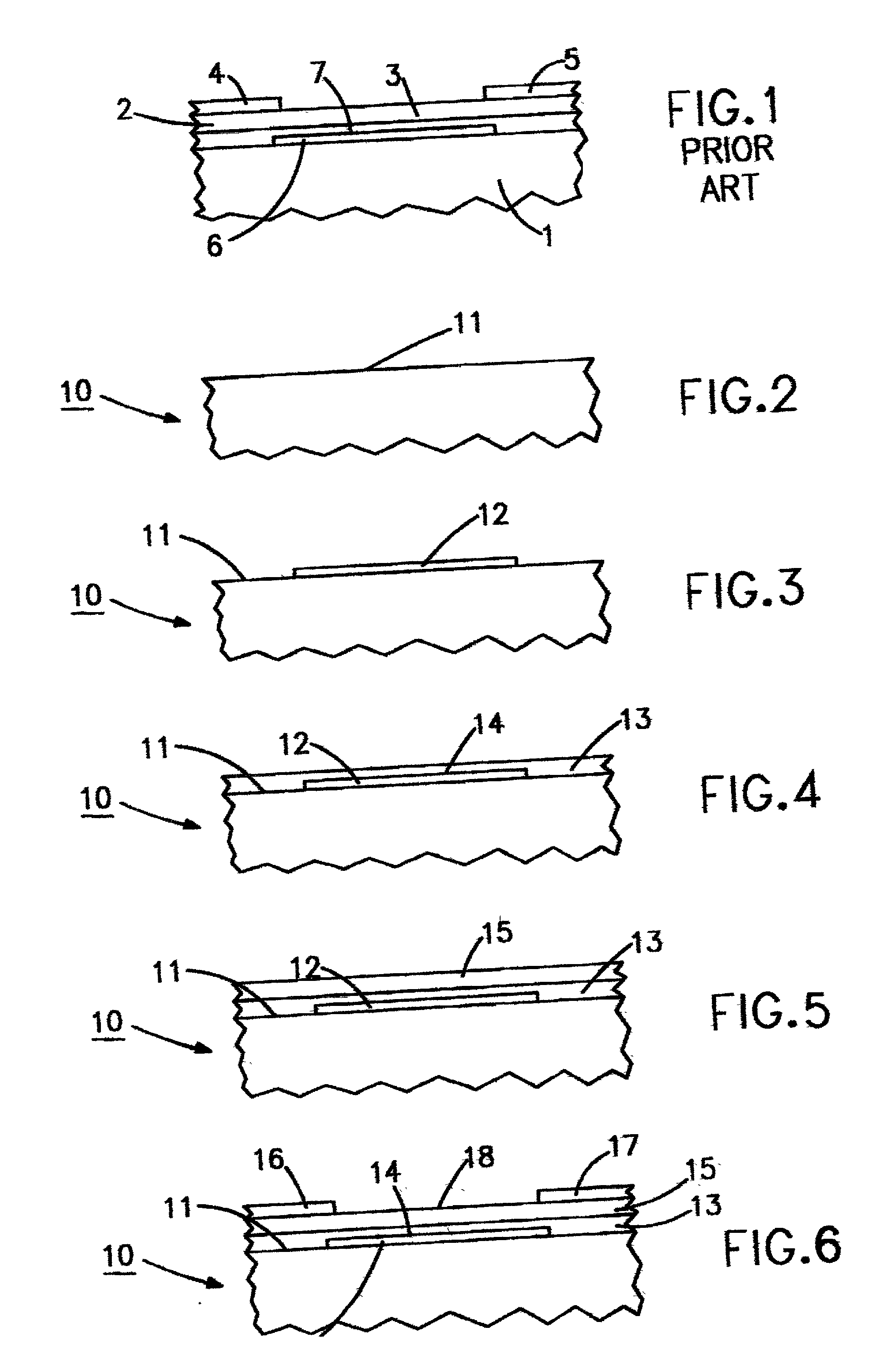
[0044] TFT's having as gate insulator a thin film of barium zirconate titanate (BZT), are fabricated by means of room temperature vicinity type rf sputtering as described in Example 1 together with the TFT fabrication steps described in connection with FIGS. 2-6. In this particular example, oxidized silicon substrates are cleaned in an isopropanol bath using ultrasonic agitation and dried with nitrogen. They are then assembled with a metal mask with openings corresponding to the gate lines and placed and pumped down to high vacuum in an electron beam evaporator. Gate metallization of either 400 .ANG. of aluminum or a bilayer of 150 .ANG. of titanium followed by 300 .ANG. of platinum is deposited on the substrates by electron beam evaporation. Then a gate insulator film 13 of BZT is deposited on top of the gate 12 and the substrate surface 11, as described in example 1.

[0045] An organic semiconductor pentacene layer 15 is deposited on the BZT gate insulator 13 using thermal evaporati...

example 3

[0052] TFT devices are fabricated on transparent polycarbonate substrates that are 0.020" thick which is about 0.5 mm using a sputtered BZT gate insulator that is about 1280 .ANG. in thickness deposited by the sputtering process as described in connection with FIG. 7 and using the steps described in connection with FIGS. 2-6 for depositing the other layers.

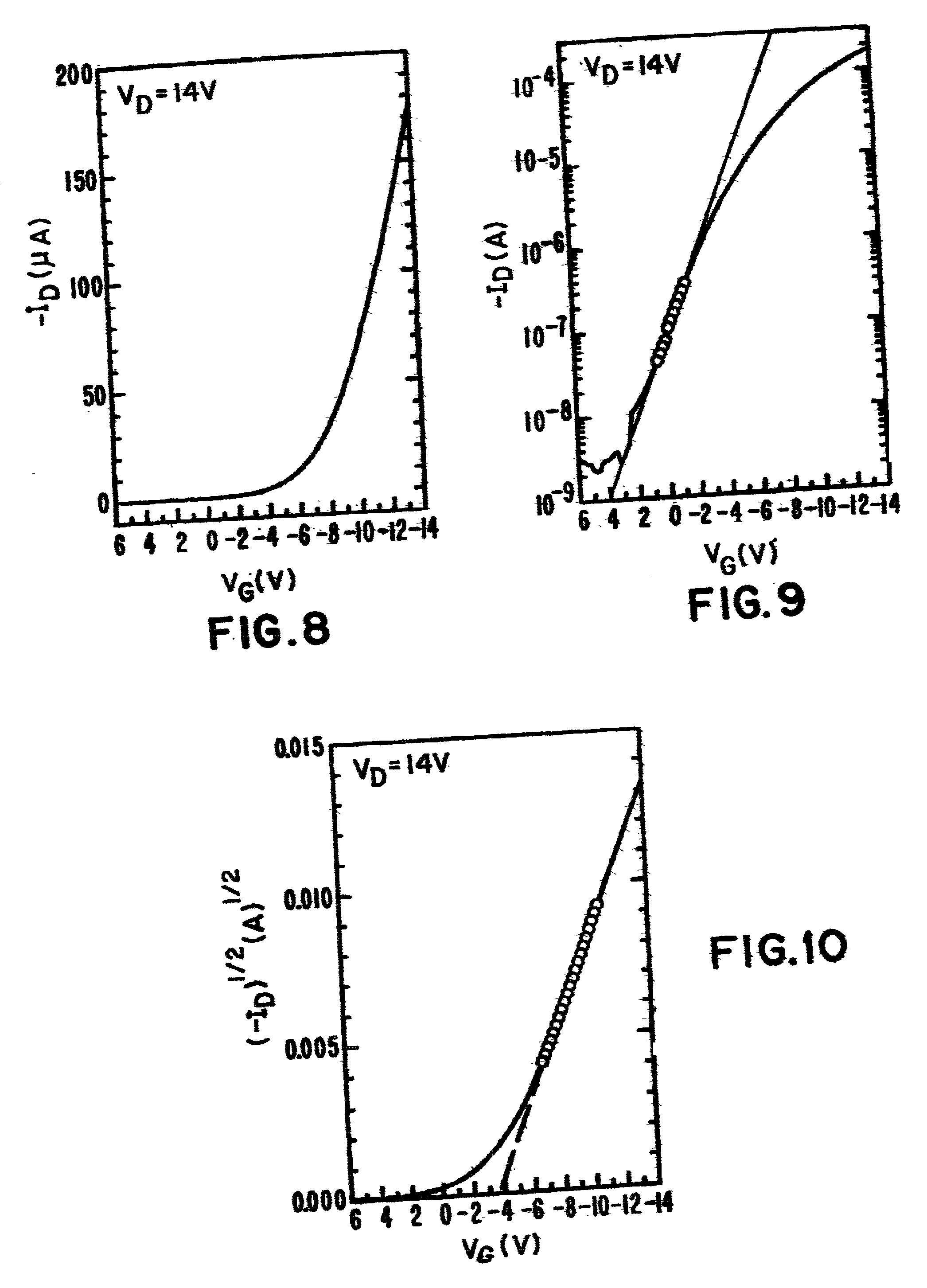
[0053] Measurements of TFT characteristics were performed as described in Example 2. Referring to FIG. 16 which shows the drain current versus drain voltage plot for a TFT device on this type of substrate with a channel length of 69 .mu.m and channel width of 1500 .mu.m. The mobility for this device was calculated to be 0.14 cm.sup.2 V.sup.-1 sec.sup.-1 while .mu.=0.20 cm.sup.2 V.sup.-1 sec.sup.-1 in the saturation regime. Mobility values as high as 0.38 cm.sup.2 V.sup.-1 sec.sup.-1 were measured from devices with a W / L ratio of 4. These are the highest reported mobilities from devices fabricated on plastic substrates, and they ar...


PUM


Abstract

The invention broadens the range of materials and processes that are available for Thin Film Transistor (TFT) devices by providing in the device structure an organic semiconductor layer that is in contact with an inorganic mixed oxide gate insulator involving room temperature processing at up to 150 degrees C. A TFT of the invention has a pentacene semiconductor layer in contact with a barium zirconate titanate gate oxide layer formed on a polycarbonate transparent substrate employing at least one of the techniques of sputtering, evaporation and laser ablation.

Description

[0001] Cross Reference is made to contemporaneous patent application Ser. No. 08 / 827,015, Filed Mar. 25, 1997, and 08 / 827,018 Filed Mar. 25, 1997; assigned to the assignee of this application; arising out of a continuing technological effort and incorporated herein by reference.FIELD OF THE INVENTION[0002] This invention pertains to thin film field effect transistors (TFT), and in particular to the structure and processing of such TFT devices at a low, of the order of 150 degrees C., or less temperature.BACKGROUND AND RELATION TO THE PRIOR ART[0003] Thin film field effect transistors (TFT), useful in flat panel display applications, at the current state of the art, involve a semiconductor layer with a channel defined by separated source and drain electrodes on one side and an insulated gate electrode on the other side that is centered with respect to the channel. The structure of the TFT device is usually fabricated through a set of serial deposition operations of carefully controll...

Claims


Application Information

Patent Timeline
Patent Type & Authority Applications(United States)
IPC IPC(8): H01L51/05H01L21/00H01L21/314H01L21/316H01L21/336H01L29/786H01L51/30H01L51/40
CPCH01L21/31691H01L51/0052H01L51/0545H10K85/615H10K10/466H01L21/02197H10K10/472
Inventor CALLEGARI, ALESSANDRO CESAREDIMITRAKOPOULOS, CHRISTOS DIMITRIOSPURUSHOTHAMAN, SAMPATH
Owner GLOBALFOUNDRIES INC
Why Eureka
Try Eureka