Nitride based transistors on semi-insulating silicon carbide substrates

Inactive Publication Date: 2001-08-30
WOLFSPEED INC
View PDF0 Cites 38 Cited by
  • Summary
  • Abstract
  • Description
  • Claims
  • Application Information

AI Technical Summary

Benefits of technology

0011] Therefore, it is an object of the present invention to provide a high electron mobility transistor (HEMT) that takes advanta

Problems solved by technology

These more familiar semiconductor materials have failed to penetrate higher power high frequency applications to the extent desirable, however,

Method used


Image

  • Nitride based transistors on semi-insulating silicon carbide substrates
  • Nitride based transistors on semi-insulating silicon carbide substrates

Examples


example

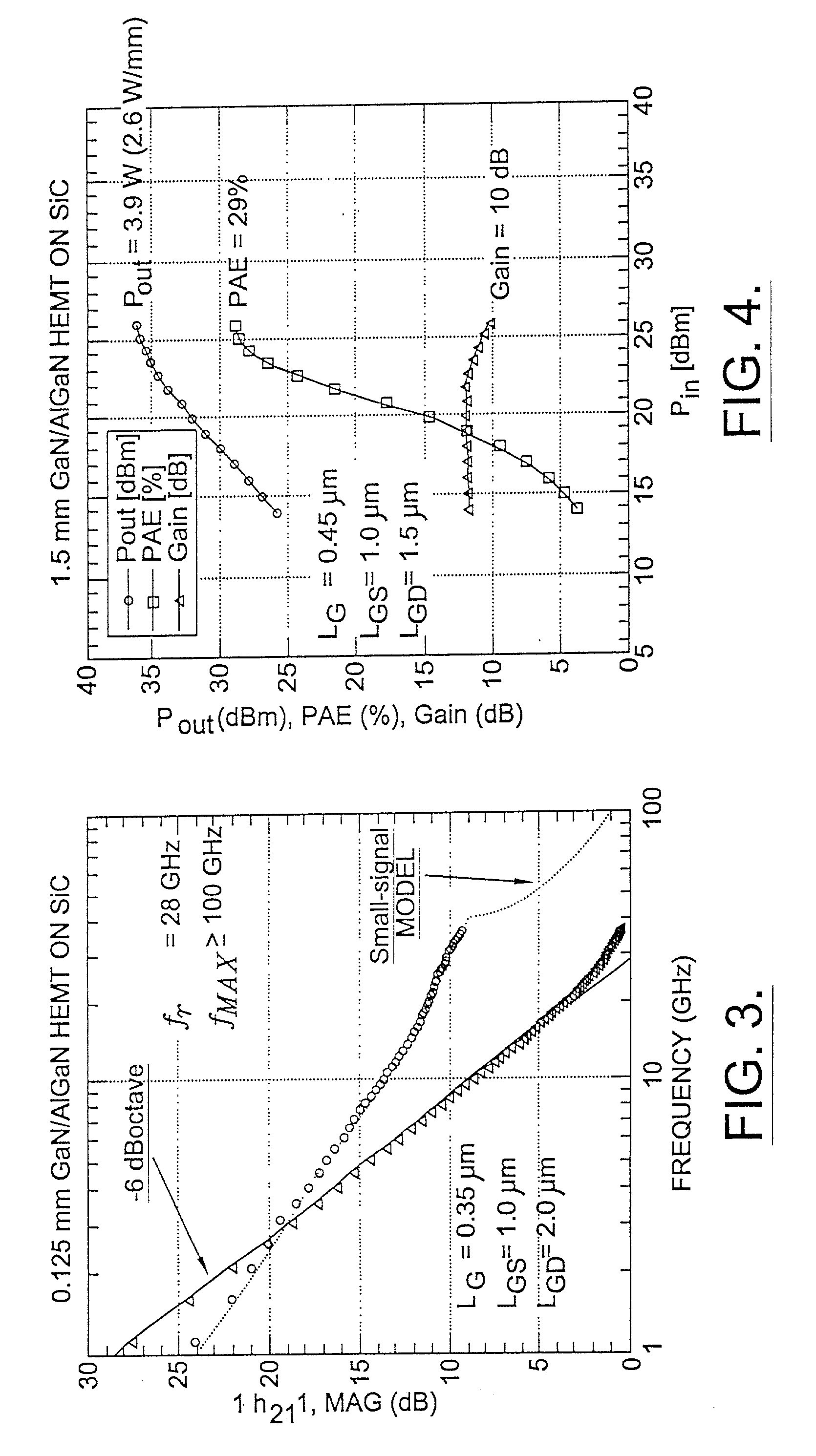
[0039] In the present invention, GaN / AlGaN HEMTs fabricated on semi-insulating 4H silicon carbide substrates have shown a total output power of 4 Watts CW (2.0 W / mm) at 10 GHz and -1 dB gain compression from a 2 mm gate width (16.times.125 .mu.m) with a power added efficiency of 29% and an associated gain of 10 dB. To date, this represents the highest total power and associated gain demonstrated for a III-Nitride HEMT at X-Band.

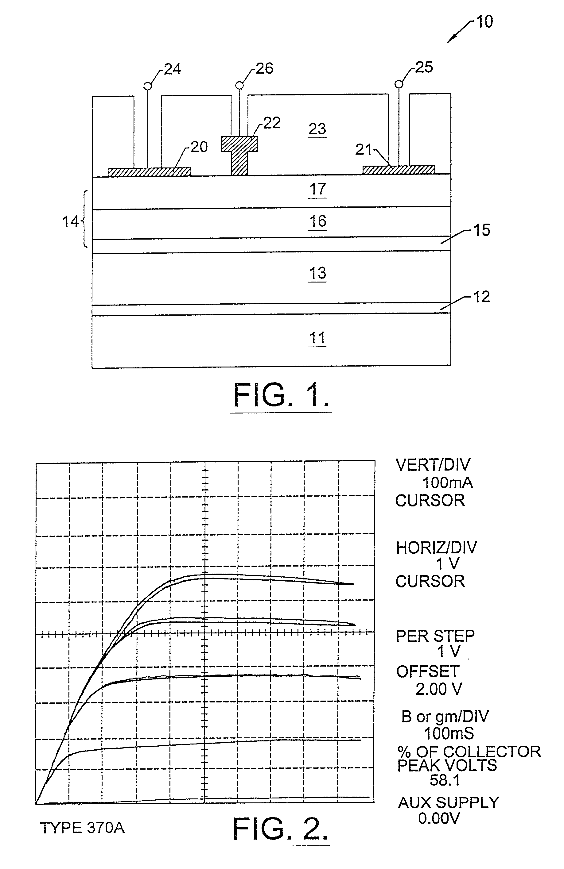
[0040] As shown in FIG. 1, the epilayer structure is comprised of an AlN Buffer Layer, 2 .mu.m of undoped GaN, and 27 nm of Al.sub.0.14Ga.sub.0.86N. The AlGaN cap has a 5 nm undoped spacer layer, a 12 nm donor layer, and a 10 nm undoped barrier layer. Device isolation was achieved with mesa etching. Ohmic contacts were Ti / Al / Ni contacts annealed at 900.degree. C. Across a 35 mm diameter SiC wafer, average values of contact resistance and sheet resistance were 0.36 Q-mm and 652 .OMEGA. / square, respectively, showing the high quality of the 2DEG over a large are...


PUM


Abstract

A high electron mobility transistor (HEMT) is disclosed that includes a semi-insulating silicon carbide substrate, an aluminum nitride buffer layer on the substrate, an insulating gallium nitride layer on the buffer layer, an active structure of aluminum gallium nitride on the gallium nitride layer, a passivation layer on the aluminum gallium nitride active structure, and respective source, drain and gate contacts to the aluminum gallium nitride active structure.

Description

BACKGROUND OF THE INVENTION[0002] The present invention relates to transistors formed of semiconductor materials that make them suitable for high power, high temperature, and high frequency applications. As known to those familiar with semiconductors, materials such as silicon (Si) and gallium arsenide (GaAs) have found wide application in semiconductor devices for lower power and (in the case of Si) lower frequency applications. These more familiar semiconductor materials have failed to penetrate higher power high frequency applications to the extent desirable, however, because of their relatively small bandgaps (e.g., 1.12 eV for Si and 1.42 for GaAs at room temperature) and relatively small breakdown voltages.[0003] Accordingly, interest in high power high temperature and high frequency applications and devices has turned to wide bandgap semiconductor materials such as silicon carbide (2.996 eV for alpha SiC at room temperature) and the Group III nitrides (e.g., 3.36 eV for GaN a...

Claims


Application Information

Patent Timeline
IPC IPC(8): H01L21/338H01L29/20H01L29/24H01L29/267H01L29/45H01L29/26H01L29/778H01L29/812
CPCH01L29/1608H01L29/2003H01L29/267H01L29/452H01L29/7783H01L29/7787H01L29/778
Inventor SHEPPARD, SCOTT THOMASALLEN, SCOTT THOMASPALMOUR, JOHN WILLIAMS
Owner WOLFSPEED INC
Why Eureka
Try Eureka