
Group-III nitride semiconductor light-emitting diode, light-emitting diode lamp, light source, electrode for group-III nitride semiconductor light-emitting diode, and method for producing the electrode

a technology of semiconductor light-emitting diodes and nitride semiconductors, which is applied in the direction of semiconductor/solid-state device manufacturing, semiconductor devices, electrical devices, etc., can solve the problems of inability to achieve stable formation of buffer layers and disadvantageous failure of upper layers to have flat surfaces, etc., and achieves small contact resistance and easy display

Inactive Publication Date: 2002-01-03
SHOWA DENKO KK
View PDF1 Cites 44 Cited by
  • Summary
  • Abstract
  • Description
  • Claims
  • Application Information

AI Technical Summary

Benefits of technology

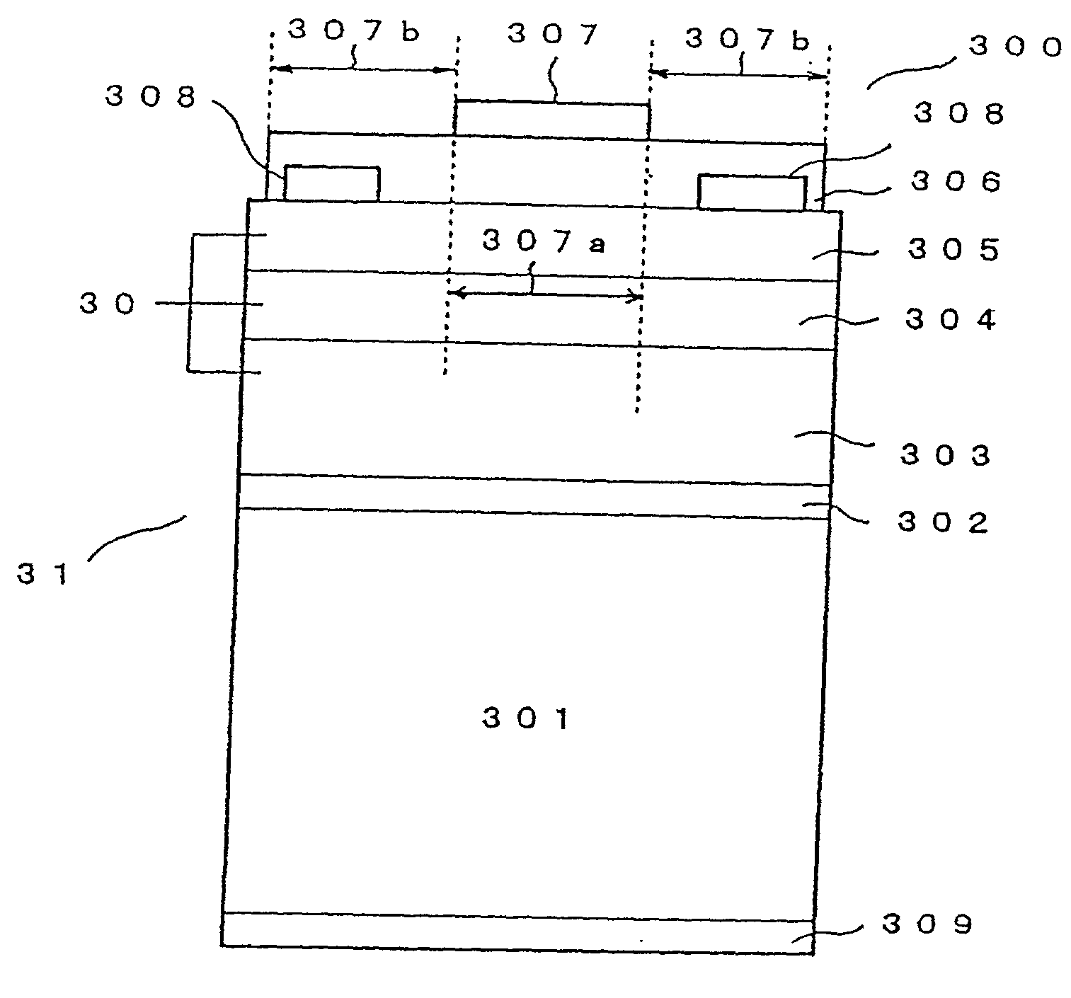
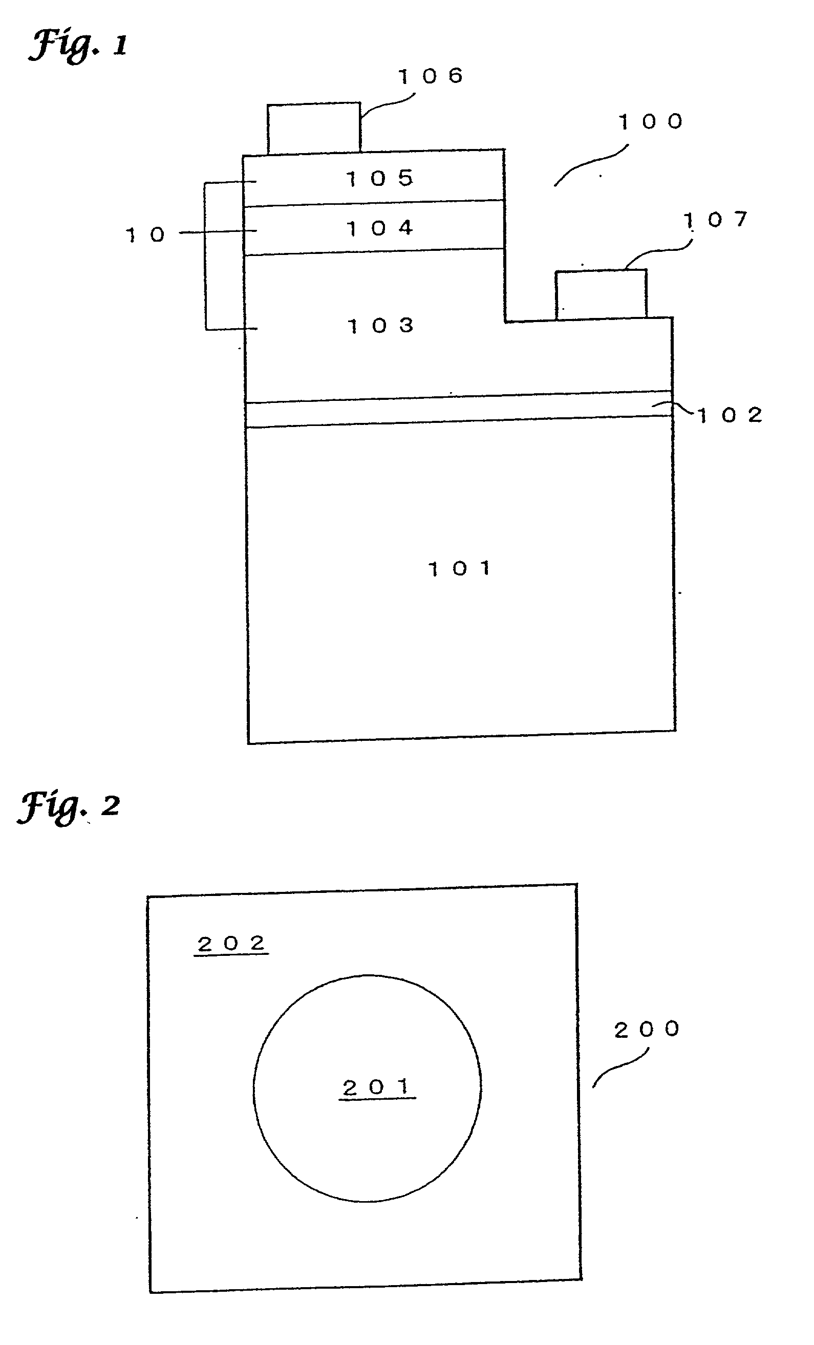
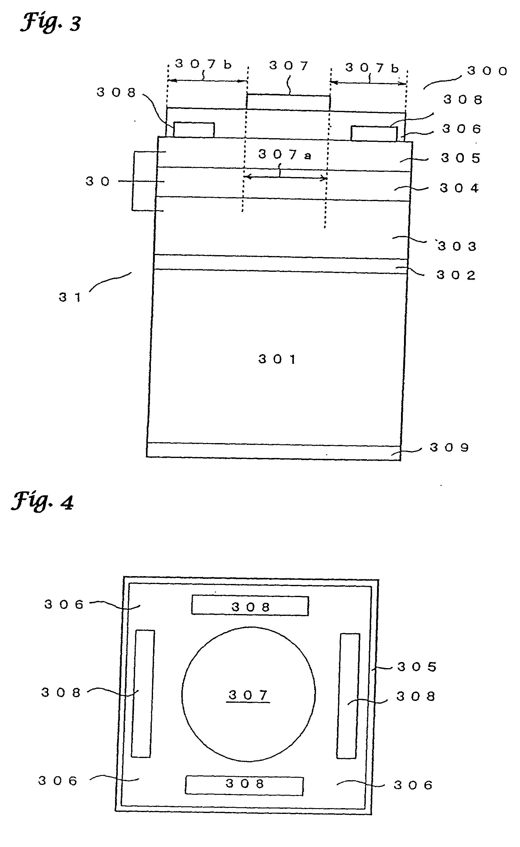
[0046] On the surface of the substrate 301 comprising an electrically conducting crystal, a buffer layer 302 composed of a boron phosphide (BP)-based material is provided. The boron phosphide (BP)-based material means a group III-V compound semiconductor containing at least boron (B) and phosphorus (P) as constituent elements. Examples of the BP-based material include boron nitride phosphide (BN.sub.1-XP.sub.X, where 0<X<1) and boron gallium phosphide (B.sub.1-YGa.sub.YP, where 0<Y<1), in addition to boron phosphide (BP). The BP-based material is reduced in the lattice mismatch with a group-III nitride semiconductor constituting the pn-junction type double hetero (DH) junction light-emitting part 30, such as gallium nitride (GaN). For example, BN.sub.0.03P.sub.0.97 (lattice constant: 4.510 .ANG.) having a nitrogen compositional ratio (=1-X) of 0.03 (3%) is advantageous in that a buffer layer capable of lattice-matching with cubic crystal GaN can be formed therefrom. By virtue of this good lattice matching, the buffer layer comprising a BP-based material exerts an effect of giving an upper layer reduced in the density of crystal defects such as misfit dislocation, and having excellent crystallinity.
[0072] The gallium nitride phosphide (GaN.sub.1-XP.sub.X, where 0<X<1) crystal layer used for the contact layer of the surface ohmic electrode can provide an effect of giving a surface ohmic electrode having a small contact resistance.

Problems solved by technology

If the film formation temperature is less than about 200.degree. C., the thermal decomposition of starting materials does not satisfactorily proceed and therefore, stable formation of the buffer layer cannot be attained.
If the growth temperature exceeds 500.degree. C., a polycrystalline layer is readily formed, and this is disadvantageous in that on the polycrystalline layer comprising randomly gathered single crystals, crystals readily grow in random azimuths by reflecting the orientation (coordinate direction) of each single crystal constituting the polycrystalline layer, and the upper layer obtained disadvantageously fails in having a flat surface.

Method used


Image

  • Group-III nitride semiconductor light-emitting diode, light-emitting diode lamp, light source, electrode for group-III nitride semiconductor light-emitting diode, and method for producing the electrode
  • Group-III nitride semiconductor light-emitting diode, light-emitting diode lamp, light source, electrode for group-III nitride semiconductor light-emitting diode, and method for producing the electrode
  • Group-III nitride semiconductor light-emitting diode, light-emitting diode lamp, light source, electrode for group-III nitride semiconductor light-emitting diode, and method for producing the electrode

Examples


example 1

[0075] FIG. 6 is a schematic plan view of a group-III nitride semiconductor LED 600 of Example 1. FIG. 7 is a schematic sectional view cut along the broken line A-A' of LED 600 shown in FIG. 6.

[0076] LED 600 was fabricated based on a stacked layer structure 61 comprising a substrate 601 having provided thereon the following layers 602 to 605:

[0077] (1) a substrate 601 composed of a boron (B)-doped Si single crystal having a p-type conductive (100) face,

[0078] (2) a low-temperature buffer layer 602 comprising a Zn-doped p-type boron phosphide (BP) and having a layer thickness of about 20 nanometer (nm), which was grown at 350.degree. C. by a normal pressure (atmospheric pressure) MOCVD method in a reaction system of triethylborane ((C.sub.2H.sub.5).sub.3B) / phosphine (PH.sub.3) / hydrogen (H.sub.2) while setting the feed ratio (V / III ratio) between PH.sub.3 and (C.sub.2H.sub.5).sub.3B to about 300,

[0079] (3) a Zn-doped p-type boron phosphide (BP) single crystal layer 603 having a layer ...

example 2

[0094] In Example 2, the present invention is described by referring to a group-III nitride semiconductor light-emitting diode 700 different in the configuration of surface ohmic electrodes 609 from Example 1 and manufactured using the same stacked layer structure 61 as in Example 1.

[0095] FIG. 8 shows a schematic plan view of a group-III nitride semiconductor LED 700 according to Example 2. In FIG. 8, the same portions as those shown in FIG. 6 are indicated by the same reference numbers as in FIG. 6 and not described here.

[0096] In the group-III nitride semiconductor LED 700 of Example 2, a frame-shaped surface ohmic electrode 609 having a stratified structure consisting of a gold (Au) lower layer and a nickel oxide (NiO.sub.X, where X is about 1) upper layer was provided on the open light-emitting region 607b in the periphery of the pad electrode 607. The outer circumference of the frame-shaped surface ohmic electrode 609 had a square form by reflecting the outer shape of the squa...

example 3

[0108] In Example 3, a group-III nitride semiconductor LED was fabricated using a stacked layer structure obtained by stacking gallium nitride phosphide (GaN.sub.1-XP.sub.X, where X=0.03) which becomes an ohmic contact layer 610, on the n-type gallium nitride (GaN) layer 605 constituting the uppermost layer of the stacked layer structure described in Example 1. FIG. 9 shows a schematic sectional view of the group-III nitride semiconductor LED according to Example 3. In FIG. 9, the same constituent elements as those shown in FIG. 7 are indicated by the same reference numbers and not described here.

[0109] The n-type gallium nitride phosphide (GaN.sub.0.97P.sub.0.03) having a phosphorus compositional ratio of 3% and constituting the ohmic contact layer 610 was grown at 980.degree. C. by a reduced-pressure MOCVD method in a reaction system of trimethylgallium ((CH.sub.3).sub.3Ga) / ammo-nia (NH.sub.3) / phosphine (PH.sub.3) / hydrogen (H.sub.2). The carrier concentration of the ohmic contact ...


PUM


Abstract

The present invention solves the problem of conventional group-III nitride semiconductor LED in that, since the LED driving current is supplied only from a pad electrode serving also as an ohmic electrode, the driving current cannot diffuse over a wide range of the light-emitting region and a group-III nitride semiconductor LED having high light emission intensity cannot be successfully provided. A group-III nitride semiconductor LED having high light emission intensity, which is fabricated using a stacked layer structure obtained by providing a surface ohmic electrode, a window layer including an electrically conducting transparent oxide crystal layer and a pad electrode on an electrically conducting substrate through a boron phosphide (BP)-based buffer layer to allow the driving current to diffuse over a wide range of the light-emitting region is provided.

Description

[0001] This application is an application filed under 35 U.S.C. .sctn.111(a) claiming benefit pursuant to 35 U.S.C. .sctn.119(e)(1) of the filing date of Provisional Application No. 60 / 248,011 filed Nov. 14, 2000 pursuant to 35 U.S.C. .sctn.111(b).[0002] The present invention relates to a group-III nitride semiconductor light-emitting diode (LED) having a configuration of ohmic electrodes suitable for diffusing a driving current of a device over a wide range of a light-emitting region, an electrode for use in the group-III nitride semiconductor light-emitting diode and a method for producing the electrode.[0003] A group-III nitride semiconductor light-emitting diode is fabricated by providing an electrode on a stacked layer structure having a pn-junction type light-emitting part comprising, for example, aluminum gallium indium nitride (Al.sub.XGa.sub.YIn.sub.1-X-YN, where 0.ltoreq.X, Y.ltoreq.1 and 0.ltoreq.X+Y.ltoreq.1). In the stacked layer structure, a buffer layer is generally p...

Claims


Application Information

Patent Timeline
Patent Type & Authority Applications(United States)
IPC IPC(8): H01L33/14H01L33/38H01L33/42
CPCH01L33/14H01L33/387H01L33/42
Inventor UDAGAWA, TAKASHI
Owner SHOWA DENKO KK
Learn More