Production of organic luminescence device

a luminescence device and organic technology, applied in the direction of electroluminescent light sources, printing, electric lighting sources, etc., can solve the problems of difficult to form organic luminescence layers in patterns, difficult to produce high-definition full-color display panels, complicated production processes

Inactive Publication Date: 2002-01-03
CANON KK
View PDF5 Cites 55 Cited by
  • Summary
  • Abstract
  • Description
  • Claims
  • Application Information

AI Technical Summary

Problems solved by technology

According to this technique, certain restrictions are present regarding mask positioning accuracy and aperture width, etc., so that it has been difficult to produce a high-definition full-color display panel.
Even the process requires vacuum deposition for forming a luminescence layer and becomes a very complicated production process.
Hitherto, it has been considered very difficult to form an organic luminescence layer in a pattern.
This is firstly attributable to a surface instability of a reflection electrode metal, so that it is difficult to form a vacuum deposition film in an accurate pattern.
Secondly, the polymer or precursor constituting the hole injection layer and organic luminescence layer are less durable against a patterning step as by photolithography.
Thirdly, an organic luminescence layer formed heretofore by patterning according to printing or ink jetting has been conventionally formed after dissolution or dilution within hydrophobic solvent, and the material deterioration is liable to be caused due to water contained in the solvent, thus resulting in a lower luminescence luminance and a lower luminescence life.
While an optimum ink viscosity can vary depending on the thickness and pattern of printed ink, and further on the surface properties of the blanket and the intaglio plate, a higher viscosity is liable to cause poor filling of the intaglio plate and leave entrapped bubbles.
While the optimum ink viscosity range can vary depending on the ink ejection scheme, it is generally difficult to eject a high-viscosity ink by an ink jet printing scheme using a relatively small ejection energy.

Method used


Image

  • Production of organic luminescence device
  • Production of organic luminescence device
  • Production of organic luminescence device

Examples


example 2

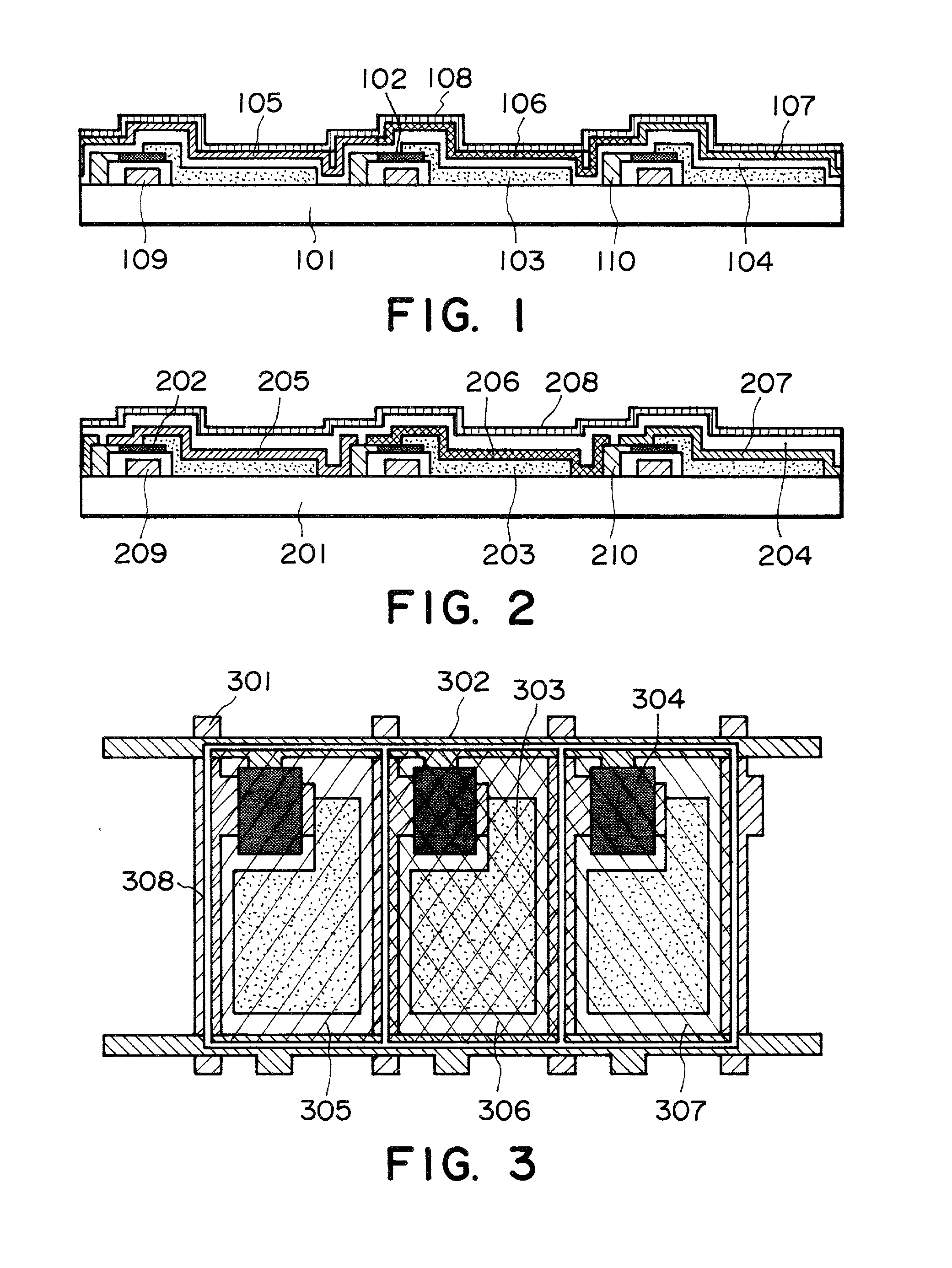
[0052] An active matrix-type organic EL full-color display panel having a planar structure also as illustrated in FIG. 3 and having a sectional structure as shown in FIG. 2 was prepared in the following manner.

[0053] As shown in FIG. 2, on a glass substrate 201, signal lines 209, gate lines 210 and thin-film transistors 202 were formed, and then AlLi alloy (Li=1 wt. %) reflection pixel electrodes 203 were formed by vacuum deposition through a mask at a vacuum of 10.sup.-5 to 10.sup.-6 torr and a deposition rate of 10 .ANG. / sec. so as to provide similar connections between the transistors and the electrodes as in Example 1.

[0054] Then, the same blue, green and red luminescence layer-forming inks as prepared in Example 1 each having a luminescent material content of 0.5 wt. % in a toluene / terpineol mixture solvent were successively applied in pattern by using an offset printing machine as illustrated in FIGS. 4A and 4B to form luminescence layers 205, 206 and 207 each in a thickness o...

example 3

[0057] An active matrix-type organic EL full-color display panel having a planar structure and a sectional structure as illustrated in FIGS. 3 and 8, respectively, was prepared in the following manner.

[0058] First, as shown in FIG. 8, signal lines 809, gate lines 810 and thin-film transistors 802 were formed on a glass substrate 801, and then ITO transparent pixel electrodes 803 were formed thereon.

[0059] Then, a partitioning wall was formed in a pattern (605 in FIG. 6) by offset printing using a system as illustrated in FIGS. 4A and 4B and a high-viscosity (4000 cps) thermosetting acrylic resin ink ("OPTOMER-SS", available from JSR K.K.), followed by heating at 60.degree. C. for 30 min., to form a 0.1 .mu.m-high partitioning wall 811.

[0060] A hole injection layer ink comprising 0.5 wt. % solution of TPA-6 in toluene was prepared in the same manner as in Example 1.

[0061] A blue luminescence layer-forming ink was prepared as a 0.5 wt. % solution in toluene of tetraphenylbutadiene ("T...

example 4

[0065] An active matrix-type organic EL full-color display panel having a planar structure and a sectional structure as illustrated in FIGS. 3 and 7, respectively, was prepared in the following manner.

[0066] First, as shown in FIG. 7, signal lines 709, gate lines 710 and thin-film transistors 702 were formed on a glass substrate 701, and then AlLi reflection pixel electrodes 703 were formed thereon. Thereafter, a 0.1 .mu.m-high partitioning wall 711 was formed by offset printing similarly as in Example 3.

[0067] Over the substrate treated above, an electron-injecting and -transporting layer-forming ink of 0.5 wt. % solution of Alq3 in toluene was applied by extrusion, followed by sufficient levelling to fill the cells (pixels) defined by the partitioning wall 711, followed by heating for evaporation of the solvent, to form a 0.05 .mu.m-thick electron-injecting and -transporting layer 704 at each pixel.

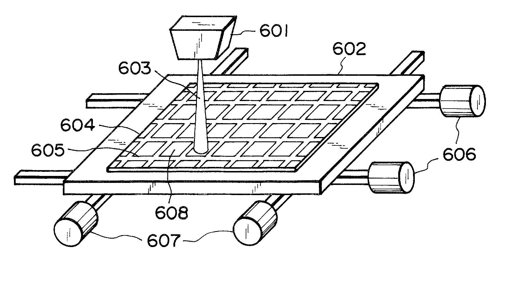
[0068] Then, by using the ink jet printing system illustrated in FIG. 6 and used in...


PUM

PropertyMeasurementUnit
melting pointaaaaaaaaaa
surface energyaaaaaaaaaa
luminanceaaaaaaaaaa

Abstract

An organic luminescence device is formed from a pair of electrodes, and a layer of organic material disposed between the electrodes so as to cause luminescence in response to a voltage applied between the electrodes. The type of organic luminescence device may be provided with improved luminescence performance if it is produced through a process including a wet-patterning step using an ink of the organic material within a hydrophobic organic solvent having a dissolving power of at most 5 wt. % of water at room temperature for producing the organic material layer.

Description

FIELD OF THE INVENTION AND RELATED ART[0001] The present invention relates to a process for producing an organic (electro-)luminescence device using a wet patterning technique, and an organic luminescence device produced by the process.[0002] An organic luminescence device (organic EL device) has a structure including a film comprising a fluorescent organic compound, and a cathode and an anode sandwiching the film. In the device, electrons and holes are injected into the film to be recombined to form excitons, and the excitons are then deactivated to cause luminescence as emission of light (fluorescence and phosphorescence) from the device.[0003] Such an organic EL device is characterized by a capability of a high-luminance planar luminescence on the order of 100-100,000 cd / m.sup.2 at a low voltage of 10 volts or below and capability of luminescence of various colors ranging from blue to red by selection of fluorescent materials.[0004] An organic EL device has called an attention fo...

Claims


Application Information

Patent Timeline
Patent Type & Authority Applications(United States)
IPC IPC(8): H01L27/32H05B33/10H01L51/00H01L51/30H01L51/40H01L51/50H01L51/56
CPCH01L27/3244H01L51/0005H01L51/0007H01L51/0035H01L51/005H01L51/0052H01L51/5012H01L51/56H10K59/12H10K71/15H10K71/135H10K85/111H10K85/60H10K85/615H10K50/11H10K71/00H05B33/10
Inventor ISHIKAWA, NOBUYUKISENOO, AKIHIROUENO, KAZUNORI
Owner CANON KK
Why Eureka
Try Eureka