Semiconductor device and manufacturing method therefor

a semiconductor and manufacturing method technology, applied in semiconductor devices, instruments, optics, etc., can solve the problems of a manufacturing process that cannot achieve 1 cm.sup.2/vsec or more, and the field mobility of silicon is small,

Inactive Publication Date: 2002-02-21
SEMICON ENERGY LAB CO LTD
View PDF7 Cites 56 Cited by
  • Summary
  • Abstract
  • Description
  • Claims
  • Application Information

AI Technical Summary

Problems solved by technology

However, the TFT in which an active layer is formed of amorphous silicon has a small field-effect mobility, i.e., a value of 1 cm.sup.2/Vsec or more cannot be obtained.
When one photomask is used, the steps of coating a resist, pre-baking, light

Method used


Image

  • Semiconductor device and manufacturing method therefor
  • Semiconductor device and manufacturing method therefor
  • Semiconductor device and manufacturing method therefor

Examples


embodiment 1

[0032] [Embodiment 1]

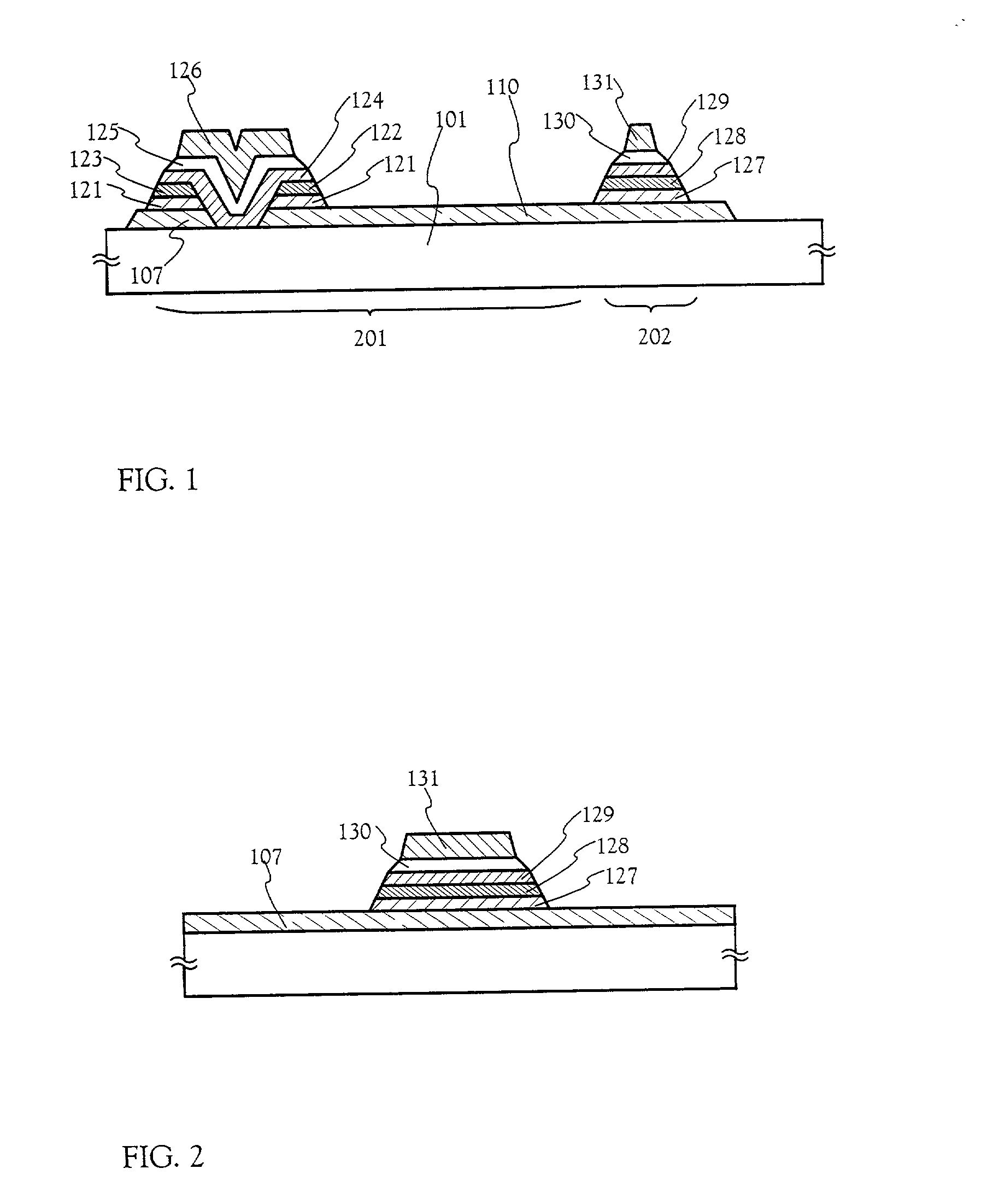
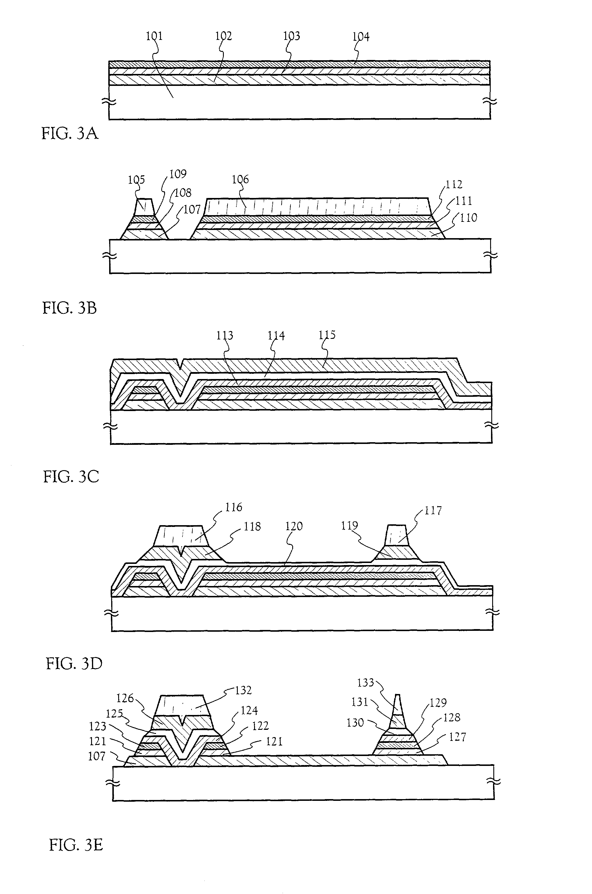
[0033] A manufacturing process of the TFT shown in FIG. 1 will be described. In FIG. 3A, as a substrate 101, a glass substrate made of barium borosilicate glass, aluminoborosilicate glass, or the like, typified by #7059 glass and #1737 glass produced by Corning Inc. can be used. Alternatively, a stainless substrate, a ceramic substrate, or the like, on which a silicon oxide film, a silicon nitride film, or the like, is formed can also be used. An organic resin substrate made of polyethersulfone (PES), polyethylene terephthalate (PET), polyethylene naphthalate (PEN), or the like can also be used.

[0034] On the substrate 101, a first conductive film 102 made of Al containing 0.1 to 2% by weight of Ti and a second conductive film 103 made of Ti are formed to a thickness of 300 nm and 100 nm, respectively, by a sputtering method. The second conductive film 103 is provided as barrier metal. An n-type first semiconductor film 104 is formed to a thickness of 80 nm, usin...

embodiment 2

[0048] [Embodiment 2]

[0049] If a transparent conductive material such as indium oxide (In.sub.2O.sub.3) or an indium oxide-tin oxide alloy (In.sub.2O.sub.3--SnO.sub.2, abbreviated as ITO) is used for the first conductive film in Embodiment 1, a transmission type liquid crystal display device can be manufactured. This is formed by using a sputtering method, a vacuum evaporation method, or the like. Etching processing of such a material is conducted by dry etching, using hydrogen iodide (HI) or hydrogen bromide (BrH). However, in particular, etching of ITO is likely to generate a residue. Therefore, in order to improve the processing property of etching, an indium oxide-zinc oxide alloy (In.sub.2O.sub.3--ZnO) may be used. An indium oxide-zinc oxide alloy has excellent surface smoothness, and thermal stability superior to that of ITO, and therefore, even when the terminal 104 is made of an Al film, a corrosion reaction can be prevented. Similarly, zinc oxide (ZnO) is also a suitable ma...

embodiment 3

[0050] [Embodiment 3]

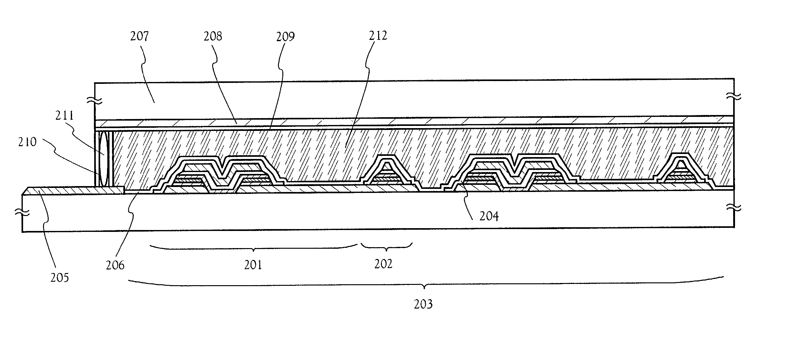
[0051] In this embodiment, a manufacturing process of an active matrix liquid crystal display device using the TFT substrate produced in Embodiment 1 will be described. As shown in FIG. 5, an orientation film 206 is formed on the TFT substrate in the state shown in FIG. 1. As an orientation film of a general liquid crystal display device, polyimide resin is mostly used. Furthermore, in FIG. 5, on the pixel TFT 201 and the storage capacitor 202 formed in a pixel portion 203, a passivation film 204 is formed using a silicon nitride film. Although the protective film 204 is important for enhancing the reliability of a TFT, it is not necessarily provided and should be appropriately provided if required.

[0052] On an opposing substrate 207 on the opposing side, a transparent conductive film 208 and an orientation film 209 are formed. Furthermore, although not shown, a light shielding film or a color filter may be formed so as to correspond to the arrangement of pixel ...


PUM


Abstract

To realize the reduction of a manufacturing cost and the enhancement of yield by reducing the number of steps of a TFT in an electro-optical device typified by an active matrix liquid crystal display device. A semiconductor device of the present invention is characterized by including a first wiring and a second wiring formed of a first conductive film on the same insulating surface, a first semiconductor film of one conductivity type formed on the first and second wirings so as to correspond thereto, a second semiconductor film formed on an upper layer of the first semiconductor film of one conductivity type across the first wiring and the second wiring, an insulating film formed on the second semiconductor film, and a third conductive film formed on the insulating film.

Description

TECHNICAL FIELD TO WHICH THE INVENTION BELONGS[0001] The present invention relates to a semiconductor device manufactured by using a thin film transistor (hereinafter, referred to as a TFT), utilizing a semiconductor film, and a method of manufacturing the same. In particular, the present invention provides a technique that is preferably applicable to an electrooptical device typified by a liquid crystal display device and an electronic device equipped with such an electro-optical device. In this specification, a semiconductor device generally refers to devices that function by utilizing semiconductor characteristics, and also includes the above-mentioned electro-optical device and electronic device equipped with the same.PRIOR ART[0002] A liquid crystal display device is utilized for displaying an image and character information in a notebook personal computer (notebook computer) and a portable information terminal. Compared with a passive liquid crystal display device, an active m...

Claims


Application Information

Patent Timeline
IPC IPC(8): G02F1/1362H01L21/77H01L21/84H01L27/01H01L27/12H01L29/04H01L29/49H01L31/036H01L31/0376H01L31/20
CPCG02F1/13458G02F1/136213G02F1/136286G02F2001/136231H01L27/124H01L27/1288H01L29/4908G02F1/136231
Inventor ARAO, TATSUYASUZAWA, HIDEOMI
Owner SEMICON ENERGY LAB CO LTD
Why Eureka
Try Eureka