
Method of producing smooth titanium nitride films having low resistivity

a technology of titanium nitride and resistivity, which is applied in the direction of vacuum evaporation coating, semiconductor/solid-state device details, coatings, etc., can solve the problems of affecting the overall conductivity of the layered conductive structure, affecting the effect of the overall conductivity of the conductive structure, and affecting the effect of the subsequent photolithographic indexing process steps

Inactive Publication Date: 2002-09-12
NGAN KENNY KING TAI +1
View PDF0 Cites 11 Cited by
  • Summary
  • Abstract
  • Description
  • Claims
  • Application Information

AI Technical Summary

Problems solved by technology

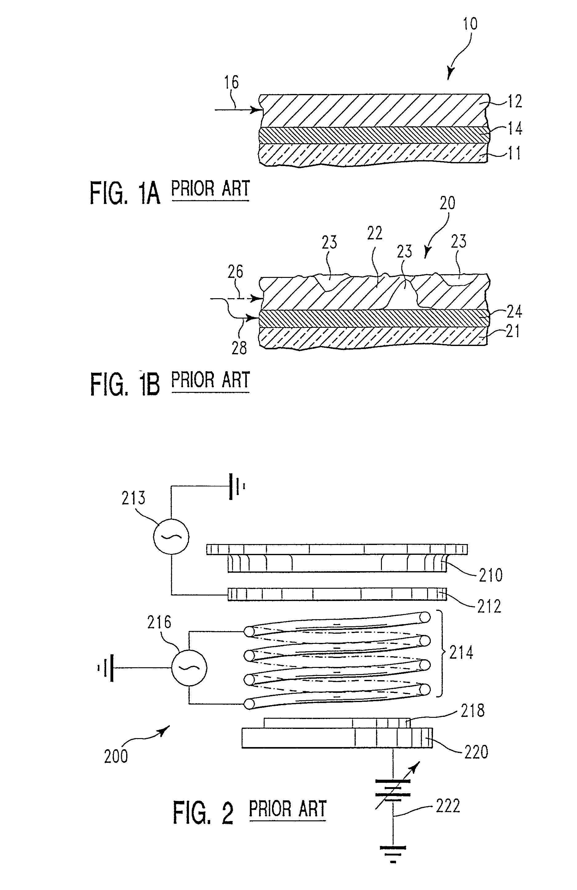
However, the resistivity of the titanium nitride, typically greater than 100 .mu..OMEGA.-cm, detracts from the overall conductivity of the layered conductive structure to which it contributes.
A rough surface on the aluminum layer makes difficult subsequent photolithographic indexing process steps necessary for formation of the overall semiconductor device structure.
The higher the ion energy, the more highly stressed the films, however.
In order to obtain optimized functionality of this barrier layer, the layer must prevent the diffusion or migration of adjacent materials through it (it must act as a barrier); it must provide high conductivity (exhibit minimal resistivity); and, it must provide a smooth surface so that other materials in the stack will not mirror surface roughness in the titanium nitride layer, thereby making subsequent lithography difficult.
However, the conductivity of an aluminum conductive layer 12 can become impaired due to stress or electromigration, which creates void structures of the kind shown in FIG. 1B.

Method used


Image

  • Method of producing smooth titanium nitride films having low resistivity
  • Method of producing smooth titanium nitride films having low resistivity
  • Method of producing smooth titanium nitride films having low resistivity

Examples


example two

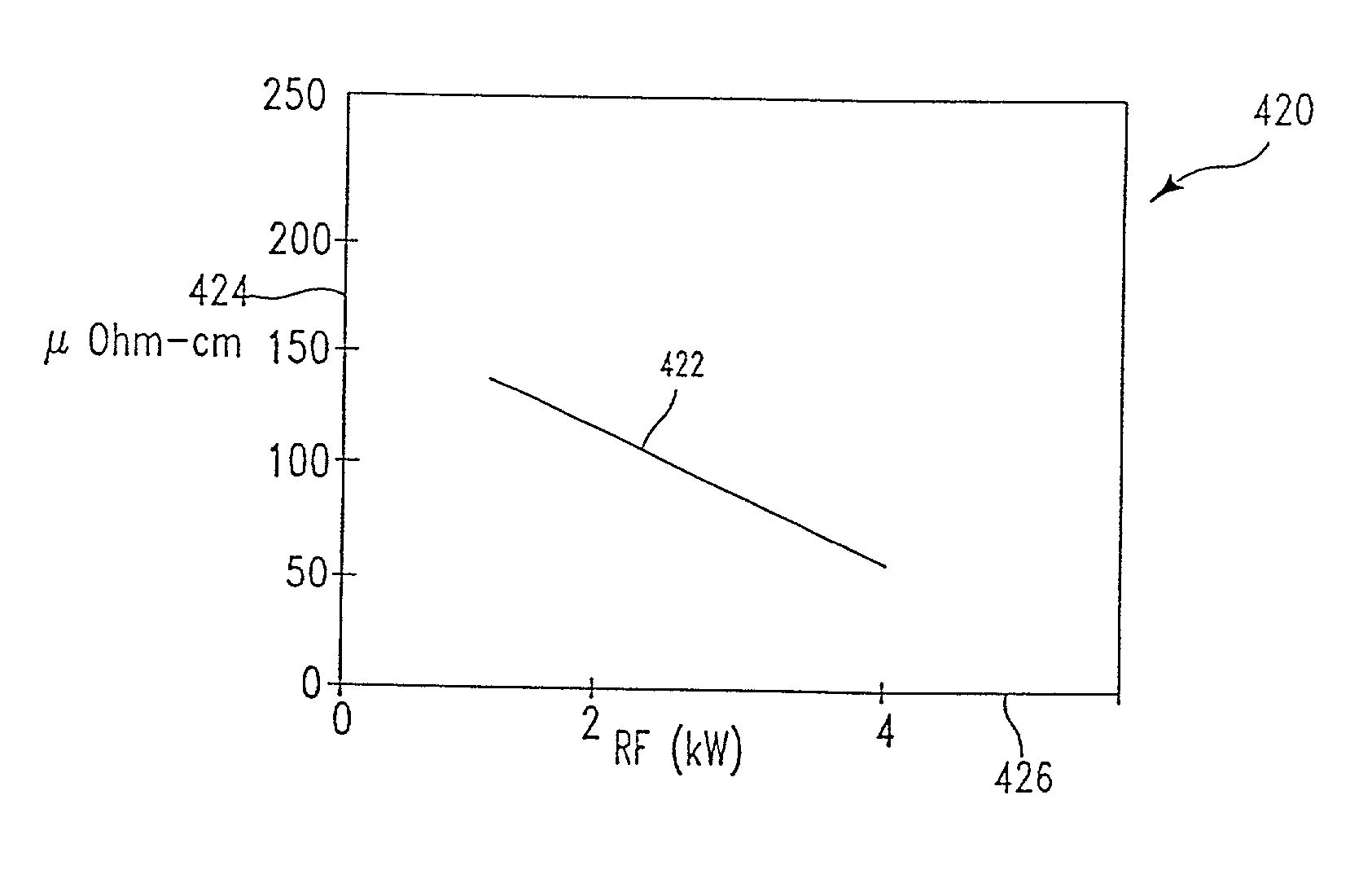
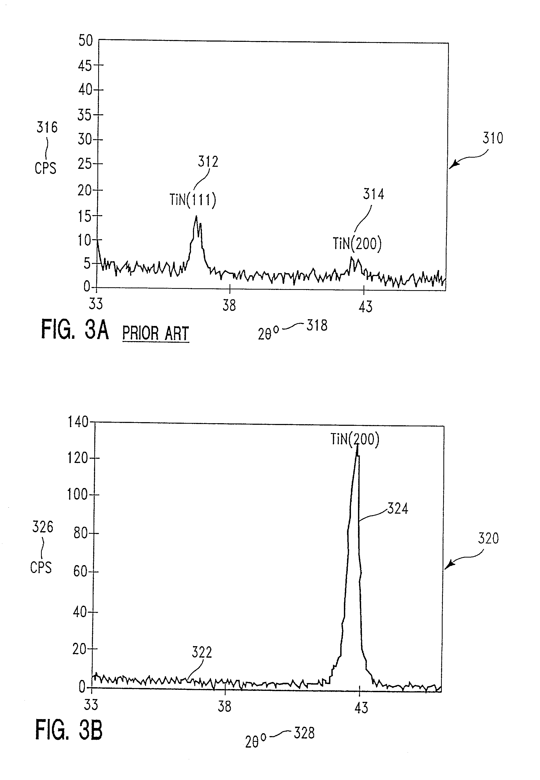
[0058] Using the equipment described above, with the DC power to sputtering target cathode 212 set at 6 kW; the coil 214 RF power set at 2 MHz and 4 kW; an argon gas flow rate of 10 sccm and a nitrogen gas flow rate of 60 sccm; with the process chamber pressure set at 25 mT; and, the substrate surface at about 300.degree. C., a 600 .ANG. thick titanium nitride film having a stoichiometric titanium nitride content, a {200} crystal orientation of about 100% and a resistivity of about 52 .mu..OMEGA.-cm was obtained.

[0059] The lower resistivity is attributed to the high {200} crystal orientation of the titanium nitride-comprising film. These physical characteristics are attributed to control of the gas phase deposition mixture composition and the quantity of the deposition mixture contacting the substrate surface over a given time period. The gas phase deposition mixture composition is believed to depend to a large extent on the DC power to the target and the RF power to the ionization ...

example three

[0070] Is Using the equipment described above, with the DC power to sputtering target cathode 212 set at 6 kW; the coil 214 RF power set at 2 MHz and 4 kW; an argon gas flow rate of 10 sccm and a nitrogen gas flow rate of 60 sccm; with the process chamber pressure set at 25 mT; and, the substrate surface at about 300.degree. C., a 600 .ANG. thick titanium nitride film having a stoichiometric titanium and nitrogen content, a {200} crystal orientation of about 100%, a resistivity of about 52 .mu..OMEGA.-cm, and a surface roughness of 0.57 nanometers (5.7 .ANG.) was obtained. Prior to the present invention, a typical surface roughness for reactive ion deposition sputtered titanium nitride films had been in the range of about 11 .ANG.. A titanium nitride film having a smoother film surface reduces any topography on the film surface which might be carried through on overlying layers, thereby improving photolithographic indexing during subsequent process steps.

[0071] To obtain a titanium ...


PUM

PropertyMeasurementUnit
temperaturesaaaaaaaaaa

Abstract

The resistivity of titanium nitride films is reduced, by about 40% (to less than about 60 muOhm-cm), for example; and, the film surface roughness is reduced, by about 45% (to less than 6 Å) by using a combination of particular process conditions during deposition of the film. In particular, titanium atoms produced by impact of inert gas ions upon a titanium target travel through a high density, inductively coupled rf plasma, an ion metal plasma (IMP), in which the titanium atoms are at least partially ionized. The ionized titanium ions are contacted with ionized nitrogen atoms also present in the processing chamber. The resultant gas phase composition is contacted with the surface of a semiconductor substrate on which a titanium nitride barrier layer is to be deposited. By controlling the gas phase deposition mixture composition, the quantity of the deposition mixture contacting the substrate surface over a given time period, and the pressure in the process vessel, the resistivity and surface roughness of the titanium nitride layer is adjusted. The resistivity of the titanium nitride barrier layer is principally determined by the crystal orientation of the titanium nitride. The more nearly the crystal orientation approaches 100% of the {200} orientation (the lower the percentage of {111} orientation), the lower the film resistivity. Crystal orientation is obtained by increasing the ionized content of the deposition mixture and by slowing the rate of deposition of the titanium nitride film (barrier layer). The surface roughness of the titanium nitride layer is reduced principally by reducing the pressure in the process vessel, which affects the film formation dynamics. An increase in ionized content of the deposition mixture helps reduce surface roughness until an inflection point is reached, after which surface roughness increases with increased ionized content.

Description

[0001] 1. Field of the Invention[0002] The present invention pertains to a titanium nitride film having a particular structure which provides a low resistivity and a smooth surface, and to the method used to create this film.[0003] 2. Brief Description of the Background Art[0004] Titanium nitride layers have been used in semiconductor device structures as barrier layers for preventing the interdiffusion of adjacent layers of materials such as aluminum and silicon, for example. However, the resistivity of the titanium nitride, typically greater than 100 .mu..OMEGA.-cm, detracts from the overall conductivity of the layered conductive structure to which it contributes. Further, if the titanium nitride surface is rough, this rough surface is mirrored in overlying layers, in an overlying aluminum layer, for example. A rough surface on the aluminum layer makes difficult subsequent photolithographic indexing process steps necessary for formation of the overall semiconductor device structur...

Claims


Application Information

Patent Timeline
Patent Type & Authority Applications(United States)
IPC IPC(8): C23C14/06C23C14/32C23C14/35H01L21/203H01L21/28H01L21/285H01L21/3205H01L21/768H01L23/52
CPCC23C14/0641C23C14/32C23C14/358H01L21/28568H01L21/76843H01L21/7685H01L21/2855
Inventor NGAN, KENNY KING-TAIRAMASWAMI, SESHADRI
Owner NGAN KENNY KING TAI
Learn More