

Method for vapor deposition of a metal compound film
a metal compound film and vapor deposition technology, applied in the direction of semiconductor/solid-state device details, coatings, transistors, etc., can solve the problems of increasing the gate leakage current, and reducing the reliability of the semiconductor devi
- Summary
- Abstract
- Description
- Claims
- Application Information
AI Technical Summary
Benefits of technology
Problems solved by technology
Method used
Image

Examples
example # 1
EXAMPLE #1
[0041] This example is directed to deposition of monoatomic layers of hafnium oxide.
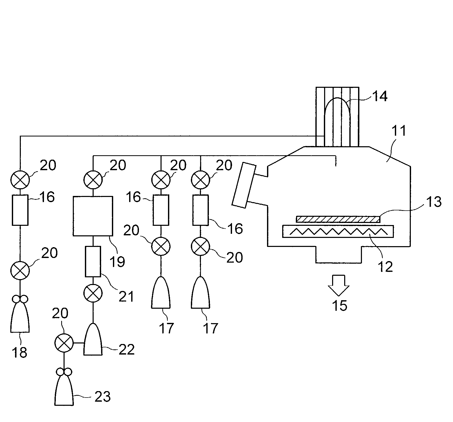
[0042] Tertiarybutoxyhafnium, i.e., Hf(OtBu).sub.4, was used as a source material of hafnium. The substrate 13 used therein was an 8-inch silicon substrate, which had thereon a thermal oxide film having a thickness of 1 nm or smaller and formed beforehand. The source material was heated up to about 80 degrees C., and introduced into the deposition chamber 11 by way of the mass flow controller 16. The partial pressure of the irradiated tertiarybutoxyed was 100 Pa, whereas the oxygen radicals were generated at an oxygen partial pressure of 1 Pa by applying thereto an electric power of 10 watts. After the substrate was heated up to 300 degrees C., the source material and the oxygen radicals were irradiated alternately in this order for 40 cycles.
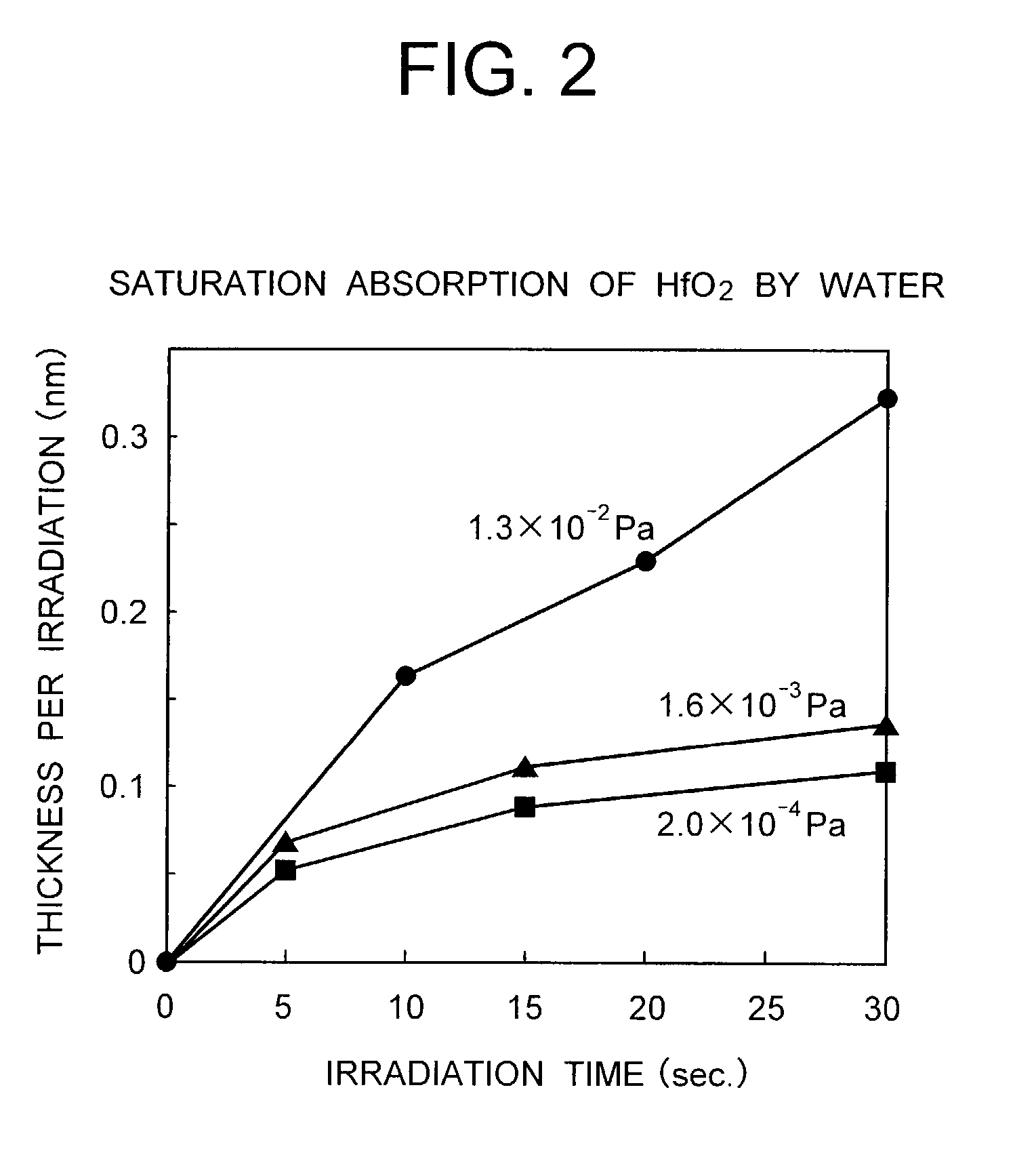
[0043] FIG. 3 shows the relationship between the film thickness deposited per each cycle of irradiation and the time length of each irradiation of the...
example # 2
EXAMPLE #2
[0054] The present example is such that the present invention is applied to using a lanthanide material. In the present embodiment, dipivaloylmethanatelanthanum (DPM of lanthanum), La(C.sub.11H.sub.19O.sub-.2).sub.3, is used as a source material for the metal compound. The DPM of lanthanum, which generally assumes the form of white powder at room temperature, was dissolved into butyl acetate at a rate of 0.1 mol. / litter to obtain a solution, which was evaporated at a rate of 0.1 gramm / min. and introduced into the deposition chamber 11 via pipe line heated up to a temperature of 200 degrees C. or above. The partial pressure of irradiated DPM of lanthanum was 100 Pa, and the oxygen radicals were generated by applying a power of 10 watts to oxygen gas at a partial pressure of 1 Pa. An 8-inch silicon substrate on which a thermal silicon oxide film had been formed beforehand was used as the substrate 13.
[0055] After heating the substrate 13 up to 300 degrees C., alternate irrad...
example # 3
EXAMPLE #3
[0058] The present example is such that the present invention is applied to deposition of monoatomic layers of Al.sub.2O.sub.3 film. FIG. 8 shows the film thickness obtained by alternate irradiation of the source material and oxygen radicals and by alternate irradiation of the source material and water, wherein the film thickness per each irradiation is plotted against the time length for the each irradiation of the source material. FIG. 9 shows the electric characteristics of the resultant Al.sub.2O.sub.3 films.
[0059] Trimethylaluminum (TMA) was used as the source material for the metal oxide in the present example, and deposited on a 8-inch silicon wafer on which a thermal oxide film having a thickness of 1 nm or less was formed. The source material was heated up to 80 degrees C. beforehand, and then introduced into the deposition chamber 11 via the mass flow controller 16. The partial pressure of irradiated trimethylaluminum was 100 Pa, and oxygen radicals were obtained...
PUM
| Property | Measurement | Unit |
|---|---|---|
| Temperature | aaaaa | aaaaa |
| Partial pressure | aaaaa | aaaaa |
| Ratio | aaaaa | aaaaa |
Abstract
Description
Claims
Application Information