Thin film bulk acoustic resonator and method of producing the same

a resonator and thin film technology, applied in the direction of generator/motor, mechanical vibration separation, instruments, etc., can solve the problems of insufficient surface roughness, difficult to increase the achievement amount of final products, and very fragile wafers

Inactive Publication Date: 2002-12-19
MEMS SOLUTIONS INC
View PDF7 Cites 146 Cited by
  • Summary
  • Abstract
  • Description
  • Claims
  • Application Information

AI Technical Summary

Problems solved by technology

However, the hole thus formed so as to penetrate through the wafer makes the wafer very fragile and easily breakable.
Further, if wet etching using KOH is carried out at an etching inclination angle of 54.7 degrees with respect to the surface of the substrate, it would be difficult to increase the achievement amount of final products, that is, to increase the yield of FBAR/SBAR on wafer.
The 0.1 .mu.m-order RMS variation is an insufficient surface roughness for the surface on which piezoelectric thin film for a thin film bulk acoustic resonator is formed.
However, the crystal is grown in various directions due to the effect of various unevenness on the rough surface, so that the crystal quality of the piezoelectric thin film achieved is not sufficient.
However, this method has many problems.
That is, since a metal layer forms a parasitic capacitor which degrades the electrical performance of the filter, it cannot be used as the layer of the Bragg reflection mirror.
Therefore, selection of materials usable for the Bragg reflection mirror is restricted.
Further, in this method, stress applied to each layer must be controlled with high precision, and thus the manufacturing process is complicated.
Further, it is difficult to form a viahole penetrating a large number of layers such as the number of 10 to 14, and thus...

Method used


Image

  • Thin film bulk acoustic resonator and method of producing the same
  • Thin film bulk acoustic resonator and method of producing the same
  • Thin film bulk acoustic resonator and method of producing the same

Examples


example 2

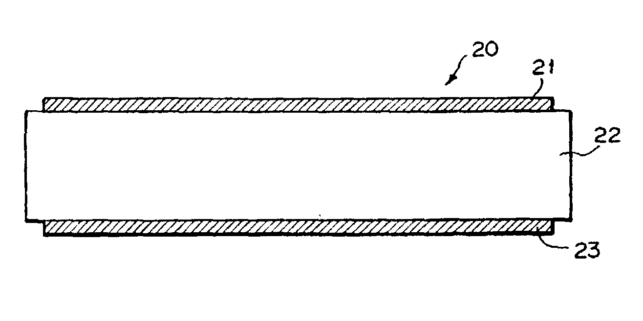
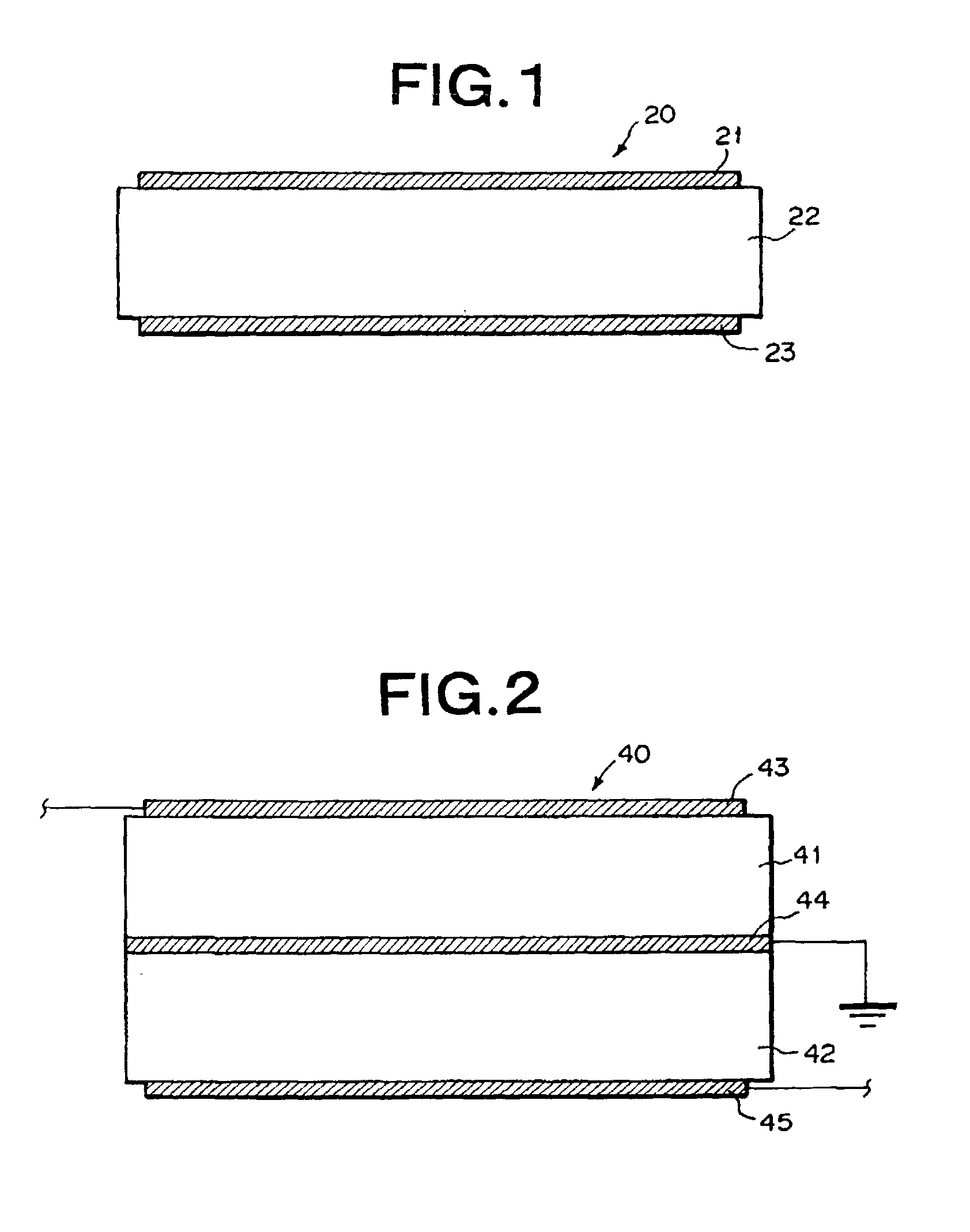
[0184] An acoustic resonator was manufactured in the same manner as EXAMPLE 1 except that AlN film was used as the piezoelectric film 62 in place of the ZnO film. That is, the piezoelectric layer 62 comprising an AlN film of 1.2 .mu.m in thickness was formed on the lower electrode 61. The formation of the AlN film was carried out by using the RF magnetron sputtering method at a substrate temperature of 400.degree. C. under the condition that Al was used as sputtering target and the mixture gas of Ar and N.sub.2 was used as sputter gas. The surface roughness of the AlN film thus formed was measured, and the result was that the RMS variation of the height was equal to 14 nm which was not more than 5% of the film thickness. With respect to the surface of the upper electrode 63, the waviness height at the measurement length of 150 .mu.m was measured, so that the it was equal to 0.2 .mu.m which was not more than 25% of the thickness of the piezoelectric layer 62 and also not more than 0....

example 3

[0191] A thin film bulk acoustic resonator was manufactured in the same manner as shown in FIGS. 3 to 5 and FIGS. 9 to 10.

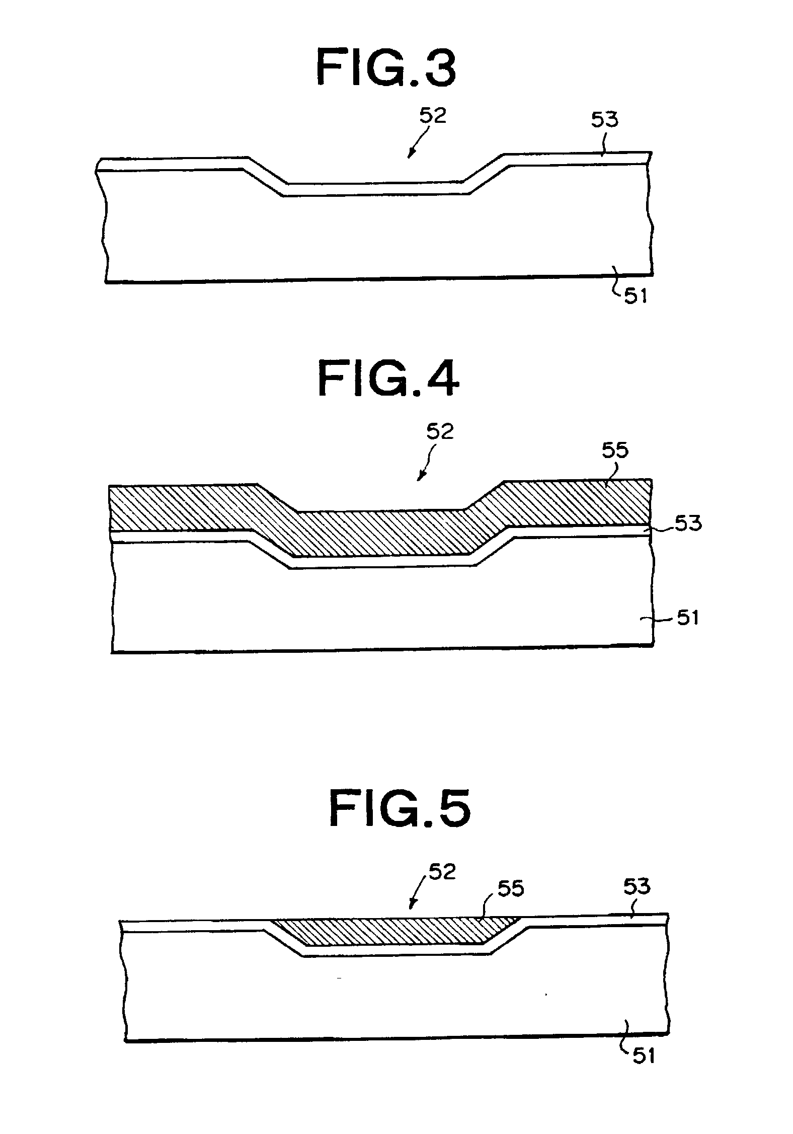
[0192] First, a structure shown in FIG. 5 was achieved in the same manner as EXAMPLE 1. However, the surface of the PSG sacrificial layer 55 remaining in the pit 52 was polished with slurry containing fine polishing particles so that the RMS variation of the height of the surface was equal to 5 nm.

[0193] Subsequently, as shown in FIG. 9, the insulating layer 54 comprising a SiO.sub.2 film of 500 nm in thickness was formed on the substrate by the CVD method so that the surface of the PSG sacrificial layer 55 was also covered by the insulating layer 54. The surface roughness of the insulating layer 54 thus formed was measured, so that the RMS variation of the height was equal to 10 nm.

[0194] Subsequently, as in the case of EXAMPLE 1, the lower electrode 61 comprising a Mo film was formed on the insulating layer 54 as shown in FIG. 10. The surface roughness of the M...

example 4

[0204] An acoustic resonator was manufactured in the same manner as EXAMPLE 2 with the exception of a manner of forming the upper electrode 63 That is, after the Mo film of 100 nm in thickness was formed on the piezoelectric layer 62 in the same manner as EXAMPLE 2, a Mo film of 20 nm in thickness was formed on the 100 nm-thick Mo film in an area extending inward from the outer edge thereof by a distance of 30 .mu.m (i.e., the width of the area is equal to 30 .mu.m) by the lift-off method, thereby forming the upper electrode 63 as shown in FIG. 11.

[0205] With respect to the surface of the center portion 631 of the upper electrode 63, the waviness height at the measurement length of 100 .mu.m was investigated, so that it was equal to 0.15 .mu.m (not more than 25% of the film thickness of the piezoelectric layer 62 and not more than 0.5% of the measurement length).

[0206] The electromechanical coupling coefficient k.sub.t.sup.2 of the acoustic resonator thus achieved was equal to 7.5%,...


PUM

PropertyMeasurementUnit
Fractionaaaaaaaaaa
Fractionaaaaaaaaaa
Fractionaaaaaaaaaa

Abstract

A pit (52) is formed in a substrate comprising a silicon wafer (51) on a surface of which a silicon oxide thin layer (53) is formed. A sandwich structure (60) comprising a piezoelectric layer (62) and lower and upper electrodes (61, 63) joined to both surfaces of the piezoelectric layer is disposed so as to stride over the pit (52). The upper surface of the lower electrode (61) and the lower surface of the piezoelectric layer (62) joined to the upper surface of the lower electrode are treated so that the RMS variation of the height thereof is equal to 25 nm or less. The thickness of the lower electrode (61) is set to 150 nm or less. According to such a structure, there is provided a high-performance thin film bulk acoustic resonator which are excellent in electromechanical coupling coefficient and acoustic quality factor.

Description

[0001] The present invention relates to a thin film bulk acoustic resonator using an electroacoustic effect of a piezoelectric thin film, and more particularly to a thin film bulk acoustic resonator usable as a constituent element of a filter for electronic circuits of communication equipment and a method of producing the same.[0002] Further, the present invention relates to a device using a piezoelectric thin film used in a broad field such as a thin film oscillator, a thin film VCO (Voltage Control Oscillator), a thin film filter, a duplexer, various kinds of sensors, etc. used in mobile communication equipment or the like.BACKGROUND TECHNIQUE[0003] In order to meet the need of reducing the cost and size of electronic equipment, an effort of reducing the size of a filter as a circuit constituent element is being made continuously without changing its way. Strict requirements on both of the size and cost of constituent parts are imposed on consumer electronic equipment such as a ce...

Claims


Application Information

Patent Timeline
IPC IPC(8): B06B1/06G10K11/04H04R19/02G10L25/90H01L41/09H01L41/22H01L41/313H03H3/02H03H9/02H03H9/05H03H9/13H03H9/17H03H9/56H03H9/58H04R31/00
CPCB06B1/0644Y10T29/49155H03H3/02H03H9/02094H03H9/02102H03H9/02149H03H9/173H03H9/174H03H9/562H03H9/564H03H9/585H03H9/587H03H2003/021H03H2003/0428Y10S977/888Y10T29/42G10K11/04H03H9/54
Inventor YAMADA, TETSUONAGAO, KEIGOHASHIMOTO, CHISEN
Owner MEMS SOLUTIONS INC
Why Eureka
Try Eureka