This transition is driven by both the increasing
impact of the RC interconnect
delay on device speed and by the
electromigration (i.e., the
mass transport of
metal due to
momentum transfer between conducting electrons and diffusing
metal atoms, thereby affecting reliability) limitations of aluminum based conductors for sub 0.25 .mu.m device generations.
Two major challenges exist for
copper wiring technology: the barrier and seed layers.
This
diffusion may lead to electrical leakage between metal wires and poor device performance.
The dielectric material can be a low dielectric constant, i.e. low-k material (used to reduce inter- and intra-line
capacitance and cross-talk) which typically suffers from poorer adhesion characteristics and lower
thermal stability than traditional
oxide insulators.
A discontinuity in the seed layer will lead to sidewall voiding, while gross overhang will lead to pinch-off and the formation of top voids.
However, as device geometries have decreased, the step coverage limitations of PVD have increasingly become an issue since it is inherently a line-of-
sight process.
As a result, PVD is unable to deposit thin continuous films of adequate thickness to coat the sides and bottoms of high
aspect ratio trenches and vias.
Moreover, medium / high-density
plasma and ionized PVD sources developed to address the more aggressive device structures are still not adequate and are now of such complexity that cost and reliability have become serious concerns.
Unfortunately, CVD requires comparatively high deposition temperatures, suffers from high
impurity concentrations, which
impact film integrity, and have higher cost-of-ownership due to long
nucleation times and poor precursor gas utilization efficiency.
This generally leads to high film resistivities (up to several orders of magnitude higher than PVD), and other degradation in film performance.
These deposition temperatures and
impurity concentrations make CVD Ta and TaN unusable for
IC manufacturing, in particular for copper metallization and low-k integration.
Although the
deposition temperature has been reduced by increased fragmentation (and hence increased reactivity) of the precursor gases in the gas-phase via a
plasma, the same fragmentation leads to the deposition of unwanted impurities.
Gas-phase fragmentation of the precursor into both desired and undesired species inherently limits the
efficacy of this approach.
In practice, ALD is complicated by the painstaking selection of a process temperature
setpoint wherein both: 1) at least one of the reactants sufficiently adsorbs to a
monolayer and 2) the surface deposition reaction can occur with adequate growth rate,and film purity.
If the temperature is too low, the deposition reaction may be incomplete (i.e., very slow), not occur at all, or lead to poor film quality (e.g.,
high resistivity and / or high
impurity content).
Since the ALD process is entirely thermal, selection of available precursors (i.e., reactants) that fit the temperature window becomes difficult and sometimes unattainable.
Due to the above-mentioned temperature related problems, ALD has been typically limited to the deposition of semiconductors and insulators as opposed to metals.
However, halides (e.g., Cl, F, Br) are corrosive and can create reliability issues in metal interconnects.
Chlorine is a corrosive, can
attack copper, and lead to reliability concerns.
Unfortunately, due to the temperature conflicts that plague the ALD method and lack of kinetically favorable second reactant, serious compromises in process performance result.
Although REALD results in a lower operating substrate temperature than all the aforementioned techniques, the process still suffers from several significant drawbacks.
Such temperatures are still too high for some films of significant interest in
IC manufacturing such as
polymer-based low-k dielectrics that are stable up to temperatures of only 200.degree. C. or less.
Moreover, a porous or under-dense film has lower
chemical stability and can react undesirably with overlying or underlying films, or with
exposure to gases commonly used in IC manufacturing processes.
Another limitation of REALD is that the radical generation and delivery is inefficient and undesirable.
RF
plasma generation of radicals used as the second reactant such as atomic H is not as efficient as
microwave plasma due to the enhanced efficiency of
microwave energy transfer to electrons used to sustain and dissociate reactants introduced in the plasma.
Furthermore, having a downstream configuration whereby the radical generating plasma is contained in a separate vessel located remotely from the main chamber where the substrate is situated and using a small aperture to introduce the radicals from the
remote plasma vessel to the main chamber body significantly decreases the efficiency of transport of the second radical reactant.
In the case of atomic H, these recombination pathways will lead to the formation of diatomic H.sub.2, a far less effective
reducing agent.
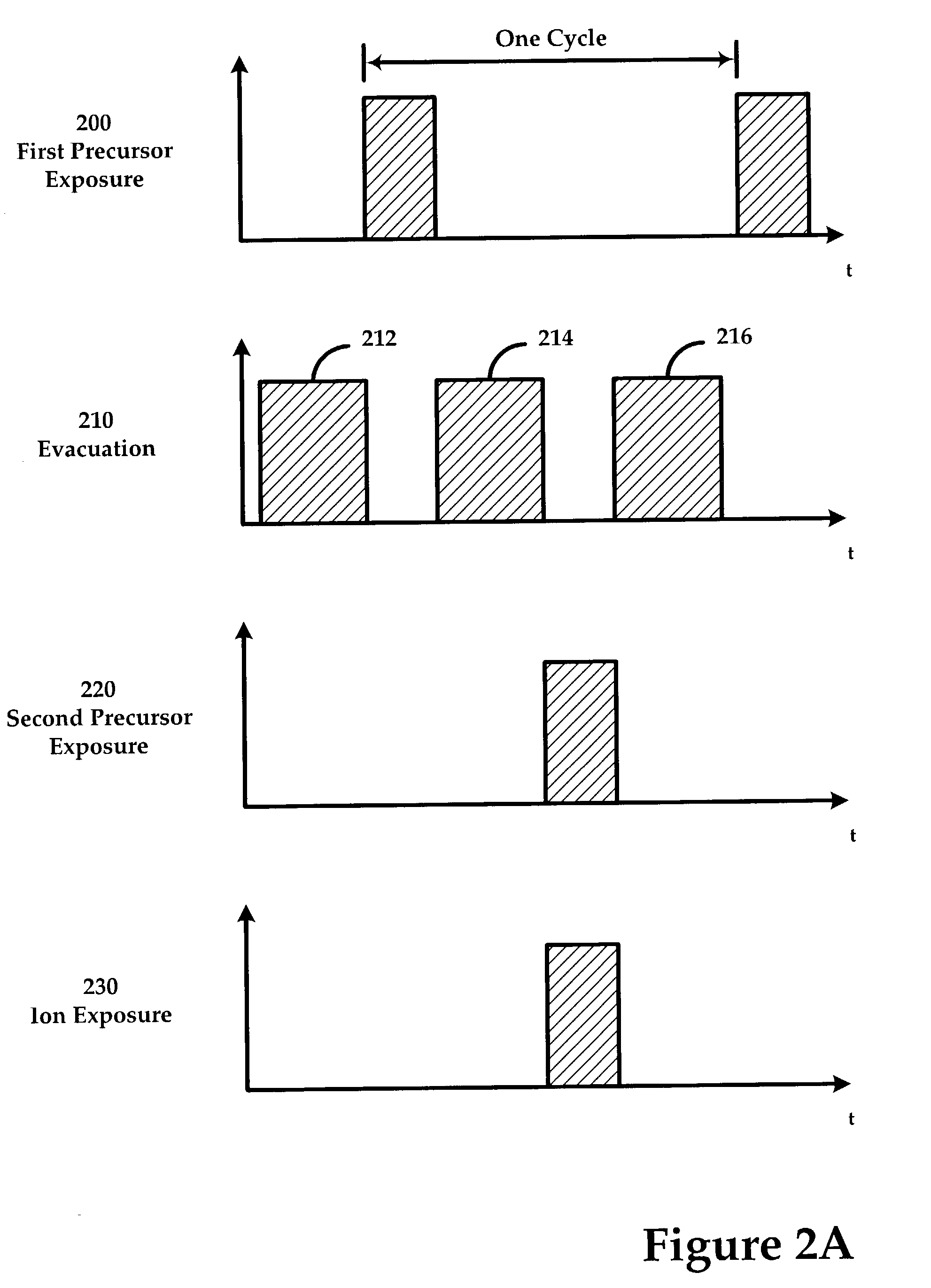
Finally, ALD (or any derivative such as REALD) is fundamentally slow since it relies on a sequential process whereby each deposition cycle is comprised of at least two separate reactant flow and evacuation steps, which can occur on the order of minutes with conventional valve and chamber technology.

