Semiconductor wafer and production method therefor

a technology of semiconductor wafers and production methods, applied in the direction of polycrystalline material growth, crystal growth process, chemically reactive gas, etc., can solve the problems of reducing productivity, increasing production cost, and resistivity reduction, so as to reduce resistivity, high resistivity, and the effect of resistivity reduction

Inactive Publication Date: 2003-01-02
SHIN-ETSU HANDOTAI CO LTD
View PDF0 Cites 7 Cited by
  • Summary
  • Abstract
  • Description
  • Claims
  • Application Information

AI Technical Summary

Benefits of technology

[0020] In such a manner, in a semiconductor wafer relating to the invention, a semiconductor thin film of 8% or less in resistivity distribution along a diameter is formed on a main surface even of a p-type semiconductor single crystal substrate as large as from 300 mm to 400 mm, both limits being included, in diameter and as low as from 0.01 .OMEGA..multidot.cm to 0.02 .OMEGA..multidot.cm, both limits being included, in resistivity, and thereby a large diameter and a uniform resistivity distribution as characteristics of a recent semiconductor wafer are both achieved, which contributes largely to increase in throughput and yield of semiconductor chips in production.
[0035] Further, in a case where a semiconductor single crystal substrate of a low resistivity lower than 0.01 .OMEGA..multidot.cm is used, since an influence of the auto-doping phenomenon increases and reduction in resistivity in the vicinity of the outer periphery of a semiconductor single crystal thin film caused by an increased influence is too sharp, simple stoppage of supply of a dopant gas onto area in the vicinity of the outer periphery of the semiconductor single crystal thin film from a gas inlet port is hard to exert a sufficient effect to make a resistivity distribution along a diameter of the semiconductor single crystal thin film uniform. On the other hand, in a case where a high resistivity semiconductor single crystal substrate of a resistivity higher than 0.02 .OMEGA..multidot.cm is used, since an influence of the auto-doping phenomenon decreases and reduction in resistivity in the vicinity of the outer periphery of a semiconductor single crystal thin film caused by the influence thereof becomes small, there arises no need for stoppage of supply of a dopant gas on to the area in the vicinity of the outer periphery from a gas inlet port, but depending on circumstances, stoppage of supply of a dopant gas onto the area in the vicinity of the outer periphery, to the contrary, has a risk to induce non-uniformity in resistivity distribution across all the semiconductor single crystal thin film. Therefore, in a case of a resistivity of a semiconductor single crystal substrate ranging from 0.01 .OMEGA..multidot.cm to 0.02 .OMEGA..multidot.cm, both limits being included, stoppage of supply of a dopant gas onto an area in the vicinity of the outer periphery of the substrate from a gas inlet port works most effectively to make a resistivity distribution along a diameter of a semiconductor thin film uniform.

Problems solved by technology

When this inventor used a silicon single crystal substrate 12 of 300 mm in diameter and a low resistivity to carry out vapor phase growth on a main surface thereof in order to respond to a recent demand for a semiconductor wafer of a large diameter, the inventor experienced a sharp reduction in resistivity in the vicinity of the outer periphery of the silicon single crystal thin film 32 due to the auto-doping phenomenon, with the result that a problem became obvious since there arose a conspicuous non-uniformity in a resistivity distribution along a diameter thereof.
In this method, however, there is a fear that a film for prevention of an auto-doping phenomenon formed on the rear main surface of the silicon single crystal substrate 12 becomes a particle generation source and / or a metal contamination source, which entails a problem of a quality of the silicon single crystal thin film 32 formed on the front main surface of the silicon single crystal substrate 12 being degraded.
In this method, in addition to an extra step of forming an auto-doping preventive film on the rear main surface of the silicon single crystal substrate 12, another extra step of removing the auto-doping preventive film after forming the auto-doping preventive film becomes necessary, which produces a problem of reduction in productivity and increase in production cost combined.

Method used


Image

  • Semiconductor wafer and production method therefor
  • Semiconductor wafer and production method therefor
  • Semiconductor wafer and production method therefor

Examples


example

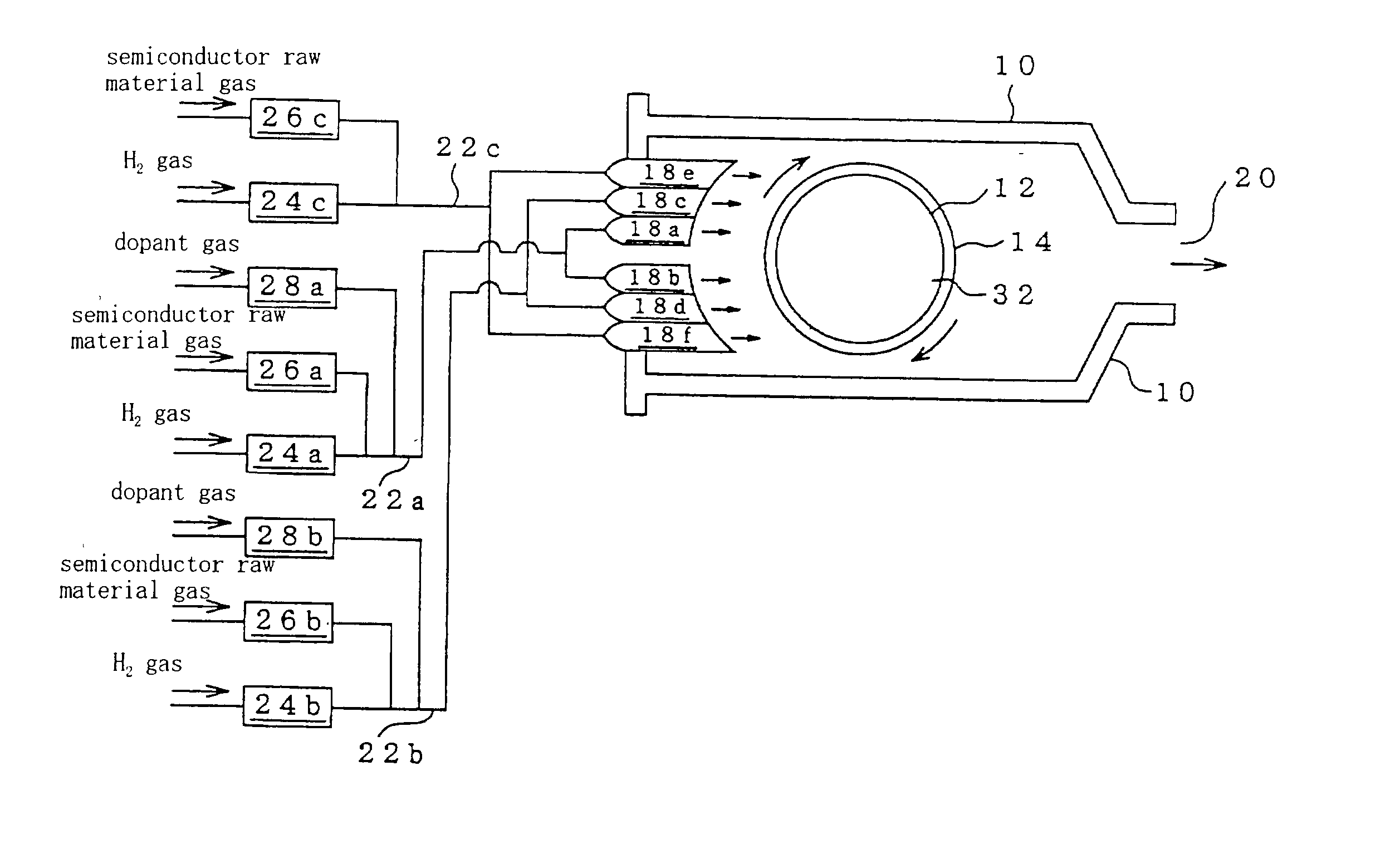
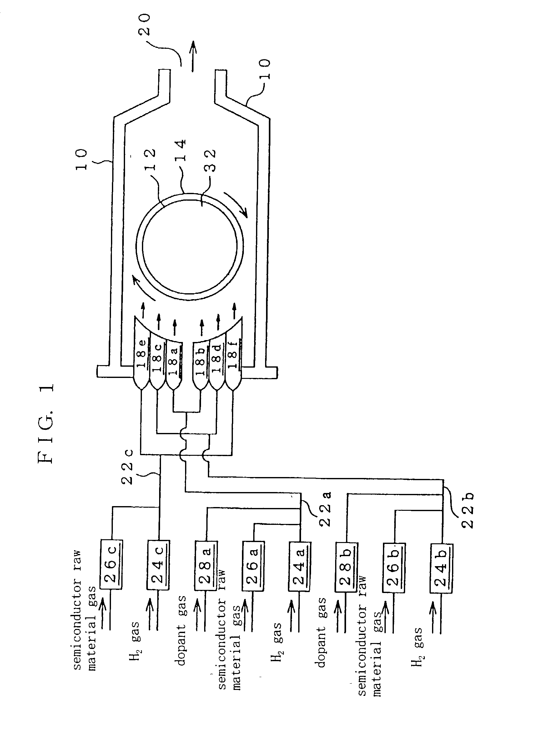
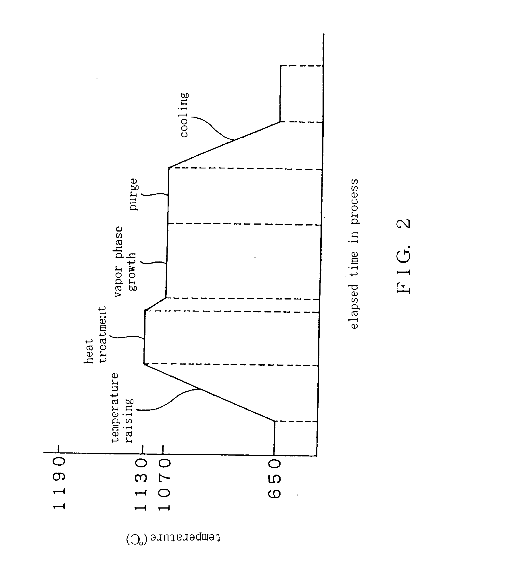
[0061] Description will be made, using FIGS. 2 and 3, of concrete operating conditions for formation of a silicon single crystal thin film on a main surface of silicon single crystal substrate using the horizontal, single wafer vapor phase growth apparatus shown in FIGS. 1 and 6, and a resistivity distribution of a silicon single crystal thin film 32 thus formed under the concrete operating conditions.

[0062] FIG. 2 is a graph showing a temperature programme in production of a semiconductor wafer using the vapor phase growth apparatus shown in FIG. 1 and FIG. 3 is a graph showing a resistivity distribution along a diameter of a semiconductor wafer produced using the vapor phase growth apparatus of FIG. 1.

[0063] As the silicon single crystal substrate 12 placed on the susceptor 14 in the reaction chamber 10, there is used a p-type low resistivity silicon single crystal substrate 12 of 300 mm.+-.0.2 mm in diameter and of a resistivity in the range of from 0.01 .OMEGA..multidot.cm to 0....


PUM

PropertyMeasurementUnit
resistivityaaaaaaaaaa
diameteraaaaaaaaaa
diameteraaaaaaaaaa

Abstract

It is an object of the invention to provide a semiconductor wafer obtained by forming a semiconductor thin film with uniform resistivity on a main surface of a semiconductor single crystal substrate of 300 mm or more in diameter. When a process gas is supplied to over a main surface of a silicon single crystal substrate 12 in rotation in almost parallel to the main surface thereof in one direction in a reaction chamber 10 through six inlet ports 18a to 18f disposed in width direction of the reaction chamber 10, H2 gas, a semiconductor raw material gas and a dopant gas are supplied onto an area in the vicinity of the center of the main surface of the silicon single crystal substrate 12 and an intermediate area thereof through the inner inlet ports 18a and 18b and the middle inlet ports 18c and 18d, and only H2 gas and the semiconductor raw material gas without the dopant gas are supplied onto an area in the vicinity of the outer periphery thereof from the outer inlet ports 18e and 18f. In such arrangement, a dopant gas produced by the auto-doping phenomenon is supplied onto the area in the vicinity of the outer periphery of the main surface of the silicon single crystal substrate 12. For this reason, the dopant gases from both sources are combined, thereby a concentration of the dopant gas supplied over all the main surface of the silicon single crystal substrate 12 is almost uniform.

Description

[0001] This invention relates to a semiconductor wafer and a production method therefor and particularly, a semiconductor wafer obtained by forming a semiconductor thin film having a uniform resistivity distribution on a main surface of a large diameter semiconductor substrate and a production method therefor.[0002] In company with recent miniaturization of an electronic device, not only has the use of semiconductor wafers each obtained by forming a silicon single crystal thin film on a main surface of a silicon single crystal substrate increased, but a more uniform resistivity distribution of the silicon single crystal thin film has also been required. The term "uniform resistivity distribution" used here, to be detailed, means that a resistivity distribution across the surface of the silicon single crystal thin film is uniform. Further, a larger diameter has also been demanded on a semiconductor wafer together with the uniform resistivity distribution. A horizontal, single wafer v...

Claims


Application Information

Patent Timeline
Patent Type & Authority Applications(United States)
IPC IPC(8): C23C16/455C30B25/02C30B25/14H01L21/205H01L21/22
CPCC23C16/455C23C16/45561C30B25/14C30B29/06Y10T29/41H01L21/02381H01L21/02532H01L21/0262H01L21/2205
Inventor OSE, HIROKI
Owner SHIN-ETSU HANDOTAI CO LTD
Why Eureka
Try Eureka