Dielectric capacitor and production process and semiconductor device

a technology of dielectric capacitors and production processes, applied in semiconductor devices, capacitors, electrical apparatus, etc., can solve the problems of film fatigue, increased coercive electric field (ec), and reduced remanent polarity, so as to suppress reactions and suppress reactions

Inactive Publication Date: 2003-02-13
NABATAME TOSHIHIDE +3
View PDF0 Cites 5 Cited by
  • Summary
  • Abstract
  • Description
  • Claims
  • Application Information

AI Technical Summary

Benefits of technology

0017] In the case where the dielectric is a ferroelectric material, said first step may be carried out at a temperature bottom than 350.degree. C. and said second step may be carried out at a temperature of 350-500.degree. C. Annealing at a temperature specified above suppresses reactions between the ferroelectric material and its adjacent electrodes. Therefore, the resulting dielectric is satisfactory and the resulting dielectric capacitor functions adequately.
0018] In the case where the dielectric is a high-dielectric material, said first step may be carried out at a temperature bottom than 250.degree. C. and said second step may be carried out at a temperature of 250-450.degree. C. Annealing at a temperature specified above suppresses reactions between the high-dielectric material and its adjacent electrodes. Therefore, the resulting dielectric is satisfactory and the resulting dielectric capacitor functions adequately.

Problems solved by technology

In practice, however, it frequently happens that the conventional dielectric capacitor used in the above-mentioned memory permits a low-dielectric layer or very large crystals (due to grain growth) to occur between the electrode and the dielectric thin film.
These large crystals cause leak current to flow through grain boundaries, with the result that leak current bottoms the withstanding voltage of the dielectric capacitor, preventing the application of a voltage high enough to operate the dielectric capacitor.
This transition layer leads to decreased remanent polarity (Pr), increased coercive electric field (Ec), and film fatigue, all of which deteriorate the function of the dielectric capacitor.

Method used


Image

  • Dielectric capacitor and production process and semiconductor device
  • Dielectric capacitor and production process and semiconductor device
  • Dielectric capacitor and production process and semiconductor device

Examples


example 2

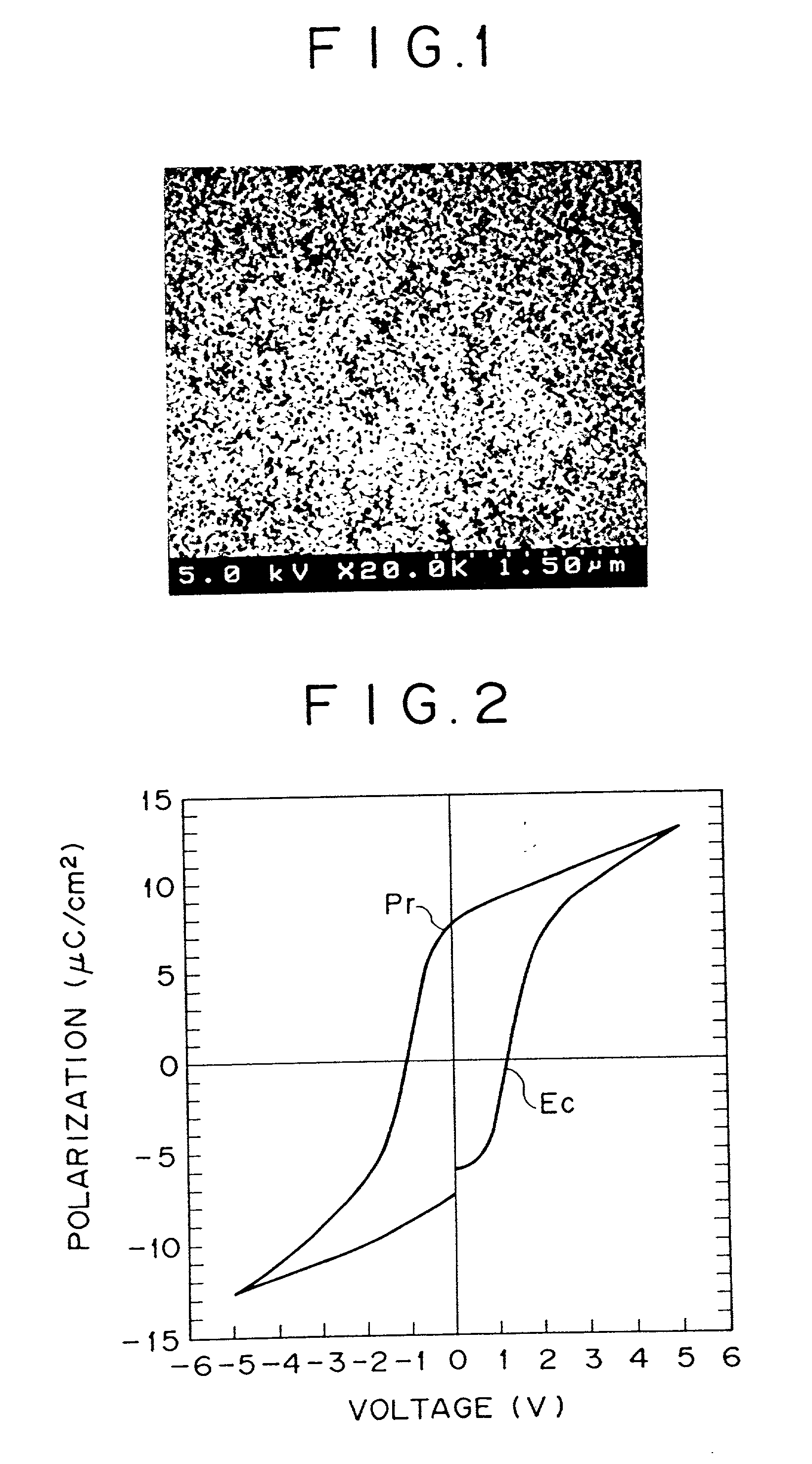
[0066] This example demonstrates another ferroelectric capacitor according to the present invention. The ferroelectric capacitor has a ferroelectric thin film whose crystal structure is represented by the structural formula of Pb(Zr.sub.0.4T.sub.0.6)O.sub.3 containing K. This structural formula corresponds to (Pb.sub.1-xA.sub.x)(Zr.sub.1-yTi.sub.y)O.sub.3 where x=0 and y=0.6. The ferroelectric capacitor in this example is produced in the same way as in Example 1. That is, the ferroelectric thin film (250 nm thick) is formed on a silicon substrate coated sequentially with SiO.sub.2, TiN layer (200 .ANG. thick), and Pt layer (1000 .ANG. thick) by sputtering under the following conditions.

[0067] target: composed of 100 pbw of Pb(Zr.sub.0.4Ti.sub.0.6)O.sub.3 and 5 pbw of K.sub.2CO.sub.3 (in terms of K).

[0068] sputtering gas 1:1 mixture of oxygen and argon.

[0069] pressure: 2 Pa

[0070] RF power: 200W

[0071] The resulting ferroelectric thin film undergoes annealing condition in air or oxygen...

example 3

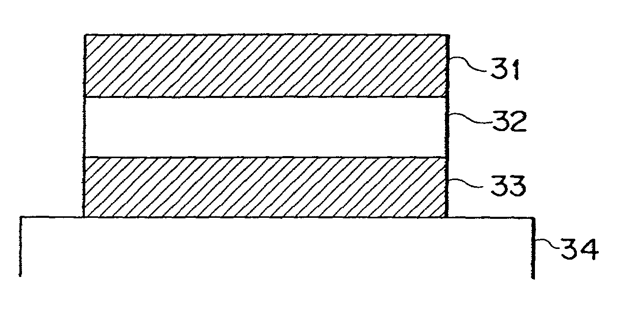
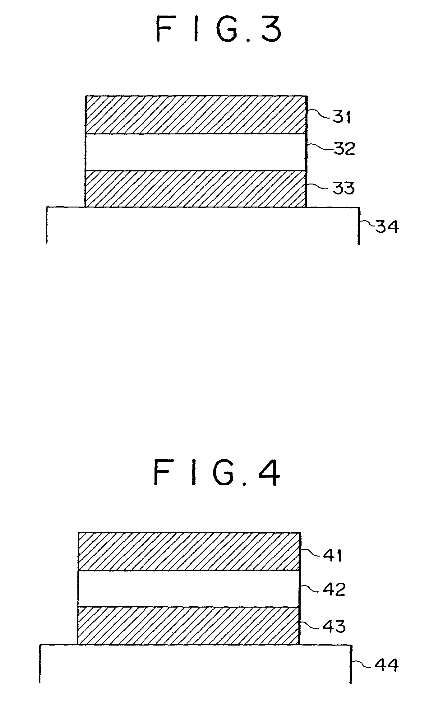
[0077] This example demonstrates a high-dielectric capacitor according to the present invention. FIG. 4 shows a schematic cross-sectional view of the high-dielectric capacitor. The high-dielectric capacitor has a high-dielectric thin film which has the crystal structure of (Ba.sub.0.5Sr.sub.0.5TiO.sub.3) containing K. The high-dielectric capacitor in this example is produced in the same way as in Example 1. The underlying substrate 44 is a silicon wafer with a TiN barrier layer (200 .ANG. thick) formed by annealing temperature at 300.degree. C. and an SiO.sub.2 layer formed by thermal oxidation. On this underlying substrate 44 was formed the bottom electrode 43 (which is a platinum thin film 200 .ANG. thick) by sputtering, with the underlying substrate kept at 350.degree. C. On the bottom electrode 43 was formed the high-dielectric thin film 42 (25 nm thick) by sputtering under the following condition.

[0078] target: composed of 100 pbw of (Ba.sub.0.5Sr.sub.0.5)TiO.sub.3 and 5 pbw of...

example 4

[0087] This example demonstrates a semiconductor device with the ferroelectric capacitor according to the present invention. FIG. 7 is a schematic sectional view of the semiconductor device. The semiconductor device is produced in the following manner. First, a silicon wafer 75 undergoes ion implantation and annealing condition so that a diffusion layer 77 is formed thereon. The surface of the substrate is oxidized to form a gate film 79 of SiO.sub.2. On the gate film 79 of SiO.sub.2 is formed a gate electrode 78. An SiO.sub.2 film 76 is formed to separate the transistor from the capacitor. A ferroelectric capacitor consisting of 73, 72, and 71 is formed. An SiO.sub.2 film 74 is formed and an aluminum interconnect 710 is formed, so that the top electrode 71 is connected to the diffusion layer 77. The ferroelectric capacitor is composed of the platinum electrode 71, the SrBi.sub.2Ta.sub.2O.sub.9 thin film 72, and the platinum electrode 73, in the same way as in Example 1. Thus there ...


PUM

PropertyMeasurementUnit
temperatureaaaaaaaaaa

Abstract

A ferroelectric material readily forms a liquid phase with an alkali metal such as Li, Na, or K (an capacitor of Group Ia) added thereto. The liquid phase reaction takes place at a bottom temperature than the solid-solid reaction. The ferroelectric material crystallizes through the liquid phase reaction. Thus it is possible to crystallize the ferroelectric material without reaction between it and its adjacent electrodes by annealing temperature at 350-500° C. which is bottom than before. Also, a ferroelectric material can be crystallized at a bottom temperature if it is added to Mg or Ca as an alkaline earth capacitor. As in the case of said ferroelectric, a high-dielectric can be crystallized at a bottom temperature (150-450° C.) if it is added to Li, Na, K, Mg, or Ca. The above-mentioned ferroelectric or high-dielectric is formed into a thin film between an top and bottom electrodes so as to produce a ferroelectric capacitor or high-dielectric capacitor.

Description

[0001] The present invention relates to a dielectric capacitor and its production process and a semiconductor device, the dielectric capacitor being one which is used as a ferroelectric capacitor (such as FeRAM) or a high-dielectric capacitor (such as DRAM).[0002] FeRAM (Ferroelectric Random Access Memory) as a non-volatile memory has a capacitor made with a ferroelectric material. It keeps its memory content even when its power supply is turned off because its ferroelectric material possesses remanent polarization. It rewrites information at very high speeds of the order of .mu.s or less. Hence, it is expected to be an ideal memory in the next generation. For a memory to have a large capacity, components constituting circuits should be finer than before. To this end, efforts are being made to reduce the capacitor size. There are several ways to achieve this object: for example, thin in the thickness of the dielectric material, utilization of a ferroelectric material with great rema...

Claims


Application Information

Patent Timeline
Patent Type & Authority Applications(United States)
IPC IPC(8): H01L21/28H01L21/316
CPCH01L21/28291H01L21/31691H01L29/40111H01L21/02192H01L21/02175H01L21/02194H01L21/02197H01L21/02356
Inventor NABATAME, TOSHIHIDESUZUKI, TAKAAKIFUJIWARA, TETSUOHIGASHIYAMA, KAZUTOSHI
Owner NABATAME TOSHIHIDE
Why Eureka
Try Eureka