
Composite ceramic board, method of producing the same, optical/electronic-mounted circuit substrate using said board, and mounted board equipped with said circuit substrate

a technology of ceramic boards and mounting boards, which is applied in the manufacture of printed circuits, high frequency circuit adaptations, basic electric elements, etc., can solve the problems of impeded operation, increased speed of operation, and inability to meet the above-mentioned modern thermal requirements or electrical requirements

Inactive Publication Date: 2003-02-20
KYOCERA CORP
View PDF0 Cites 23 Cited by
  • Summary
  • Abstract
  • Description
  • Claims
  • Application Information

AI Technical Summary

Benefits of technology

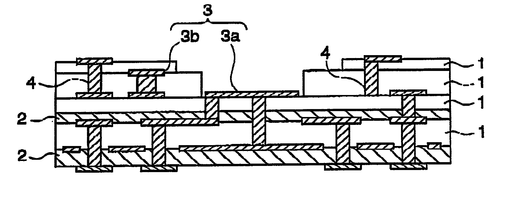
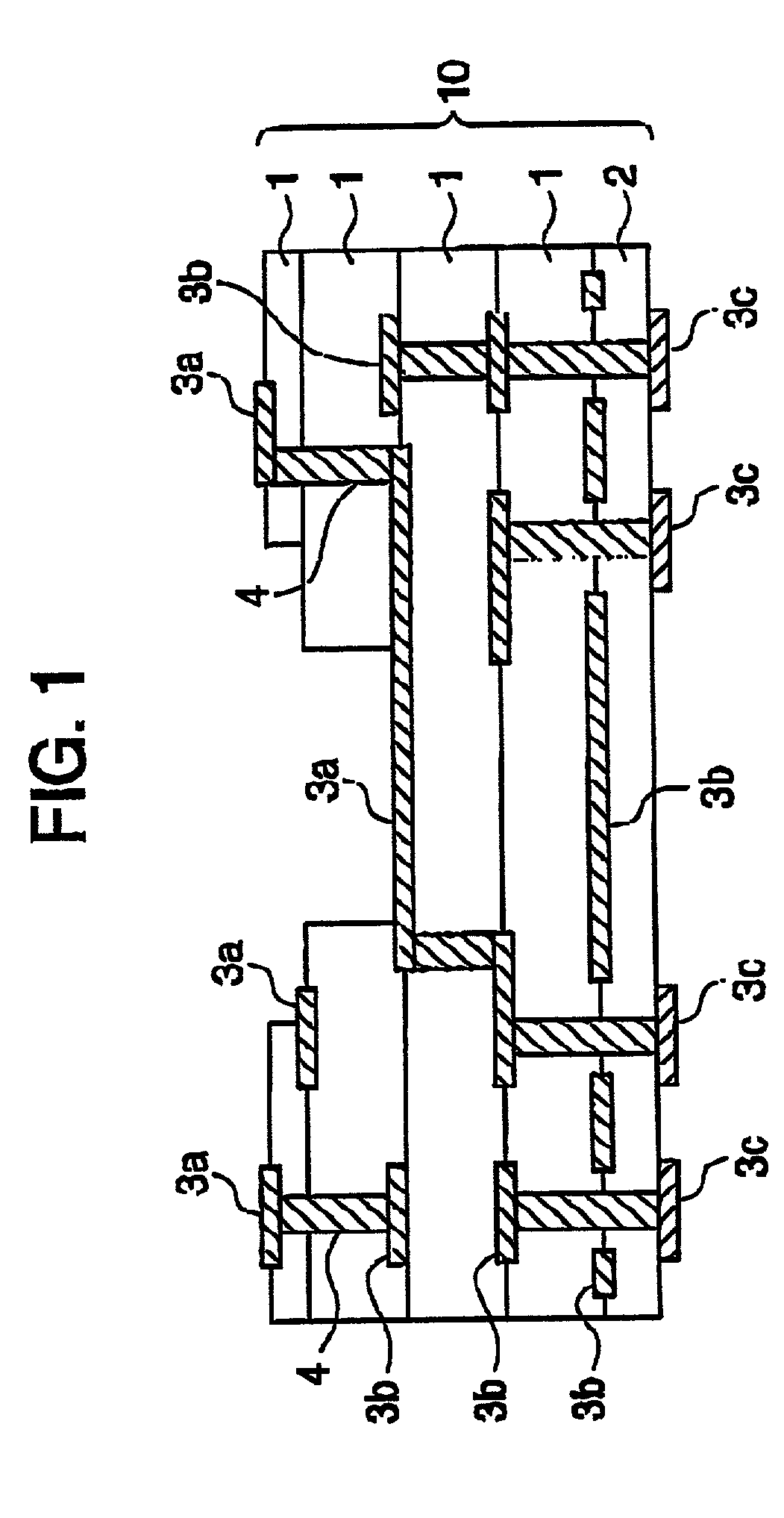
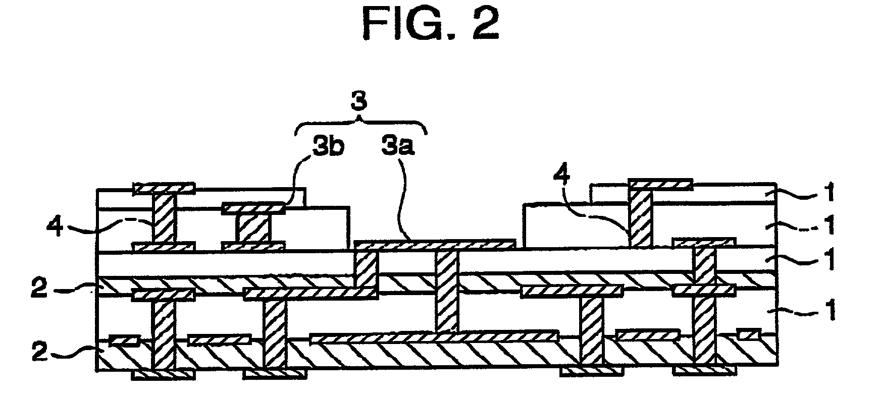
[0038] In the composite ceramic board of the present invention, an insulating board is formed by the insulating layers of alumina ceramics having a high dielectric constant and insulating layers of ceramics having a low dielectric constant which are integrally formed together by firing, to exhibit excellent properties inherent in these insulating layers.
[0080] This mounted board makes it possible to realize an optical communication which is capable of transmitting and receiving large amounts of data at high speeds.

Problems solved by technology

Further, transmitting the signals at a high frequency brings about an increase in the speed of operation, while a delay in the signals hinders the attempt for increasing the speed of operation.
However, the above-mentioned conventional ceramic board is not capable of fully meeting the above-mentioned modern thermal requirements or electrical requirements.
Therefore, signal insertion loss is very large, and favorable high-frequency characteristics are not obtained.
Besides, since the insulating board having a wiring layer serving as a terminal for receiving signals is formed of alumina ceramics having a high dielectric constant, high-frequency signals are reflected to a large degree and transmission characteristics are deteriorated.
Therefore, though high-frequency characteristics can be accomplished, heat is not smoothly radiated from the semiconductor device, and thermal properties (thermal conductivity) are not satisfactory causing the device itself to malfunction.
Besides, the insulating board has a small resistance and is cracked at the time of mounting various devices.
Therefore, a polishing step, a thick film-forming step and a thin film-forming step are indispensable for forming the surface wiring layer accompanied by such problems as an increased number of the production steps, a decreased yield and an increased cost.
In this case, the loss due to the reflection of input signals increases in a region where the signals have a frequency of about 40 GHz, resulting in a decrease in the characteristics.
The boards, however, are not satisfactory in regard to the strength since the insulating board is made of glass ceramics.
This prevents the board from being cracked when the devices are being automatically mounted and presents a drop in the yield.
That is, when the amount of aluminum oxide is smaller than the above range, the strength and thermal conductivity may decrease.
When the average particle diameter exceeds 5.0 .mu.m, on the other hand, it becomes difficult to obtain a sufficient degree of strength.
When the amount of silicon is smaller than the above-mentioned range, on the other hand, a high density is not accomplished, either, and when the amount of silicon is larger than the above-mentioned range, the thermal conductivity tends to decrease and the dielectric property tends to be deteriorated.
When the average particle diameter is not smaller than 5 .mu.m, cracks occur in the layer due to sintering and the strength of the board may decrease.
Further, the via-hole conductors 4 become rugged to a large extent and may escape during the firing.
This is because, when the amount is smaller than 0.1% by weight, the effect of addition is not obtained to a sufficient degree and when the amount exceeds 20% by weight, on the other hand, the liquid phase tends to flow out during the firing.
When use is made of a powder having an excessively large average particle diameter, it becomes difficult to adjust the average particle diameter of the chief crystal phase to lie within the above-mentioned range, and, besides, it may become difficult to conduct the firing at a temperature of not higher than 1500.degree. C. as will be described later.
Even when use is made of a powder having a too small average particle diameter, it becomes difficult to adjust the average particle diameter of the chief crystal phase to lie within the above-mentioned range and, besides, it becomes difficult to handle the powder and the cost of the powder become high.
When the average particle diameter is not larger than 0.5 .mu.m, on the other hand, it may become difficult to handle the powder.
As a result, the obtained board exhibits decreased thermal conductivity and strength.
), the high-melting point conductors such as W and Mo added to the conducting paste are sintered, and the homogeneous composition of the conductor layers 3 is not longer maintained due to fluidization of low-resistance conductor component such as Cu and, besides, the low resistance is not longer maintained.

Method used


Image

  • Composite ceramic board, method of producing the same, optical/electronic-mounted circuit substrate using said board, and mounted board equipped with said circuit substrate
  • Composite ceramic board, method of producing the same, optical/electronic-mounted circuit substrate using said board, and mounted board equipped with said circuit substrate
  • Composite ceramic board, method of producing the same, optical/electronic-mounted circuit substrate using said board, and mounted board equipped with said circuit substrate

Examples


experiment 1

[0237] A mixed powder was obtained by adding, to an aluminum oxide powder (average particle diameter of 1.8 .mu.m), 6% by weight of Mn.sub.2O.sub.3, 6% by weight of SiO.sub.2 and 0.5% by weight of MgO (the amounts of addition are all per the whole amount of the mixed powder).

[0238] To the above mixed powder were further mixed an acrylic binder and toluene to prepare a slurry thereof which was, then, molded into a green sheet for forming inner insulating layers (correspond to the alumina layers of the invention) having a thickness of 250 .mu.m by the doctor blade method.

[0239] By using mullite, forsterite, enstatite, silica, cordierite and alumina as chief components, further, the second components were prepared by mixing the chief components at ratios as shown in Table 1. The mixed powders were then molded into green sheets for forming the outer electrode-forming layer (corresponds to the low-dielectric layer of the present invention) having a thickness of 250 .mu.m in the same mann...

experiment 2

[0252] Wiring boards were produced (samples Nos. 14 to 17 and 20, 21) in the same manner as in Experiment 1 but changing the electrically conducting paste (metallizing composition) as shown in Table 1 (when two kinds of conductors were used, the volume ratio was all 1:1), and were measured in the same manner as in Experiment 1.

[0253] Further, the wiring boards were produced (samples Nos. 18 and 19) in the same manner as in Experiment 1 but changing the composition of the inner insulating layers (correspond to the alumina layers of the invention) or of the outer electrode-forming layer as shown in Table 1, and were measured in the same manner as in Experiment 1.

[0254] The results were as shown in Table 2.

1 TABLE 1 Inner insulating-layer Outer electrode-forming layer (Al.sub.2O.sub.3 layer) (low-dielectric layer) Firing Main Amount Main Amount temperature Metallising No. component (wt %) 2nd component component (wt %) 2nd component (.degree. C.) composition 1 Al.sub.2O.sub.3 87 Mn.sub...

experiment 3

[0256] As alumina layers, there were mixed an alumina powder (average particle diameter of 1.8 .mu.m), and Mn.sub.3O.sub.3 powder, an SiO.sub.2 powder, an MgO powder, a CaO powder, an SrO powder, a B.sub.2O.sub.5 powder, an Nb.sub.2O.sub.5 powder, a Cr.sub.2O.sub.3 powder and a CoO.sub.3 powder in amounts as shown in Table 3, and to which were mixed, as an organic resin for molding (binder), an acrylic binder and toluene as a solvent, to prepare a slurry thereof which was, then, molded into a sheet having a thickness of 250 .mu.m by the doctor blade method.

[0257] Via-holes were formed in the sheet at predetermined portions so as to possess a diameter of 100 to 200 .mu.m after firing.

[0258] As low-dielectric layer, further, there were mixed a forsterite powder, a cordierite powder, a Zn.sub.2SiO.sub.4 powder, an Mn.sub.2O.sub.3 powder, a CaO powder, an MgO powder, a BaO powder and a non-load.multidot.non-alkaline borosilicate glass powder in amounts as shown in Table 3, and to which ...


PUM


Abstract

A composite ceramic board comprising an insulating board of insulating layers of alumina ceramics and dielectric layers of ceramics having a dielectric constant smaller than at of said insulating layers which are fired as a unitary structure, and metallized wirings of a low-resistance conductor such as of Au, Ag, Cu or Pt formed on the surfaces and inside thereof, and a method of producing the same. The composite ceramic board not only has a large strength and a high thermal conductivity but also exhibits excellent high-frequency chararteristics and is suited for use as a high-frequency wiring board. The invention further provides an optical / electronic-mounted circuit substrate using the above board, and a mounted board having the circuit substrate of the invention connected to an electronic circuit formed on a mother board.

Description

[0001] 1. Field of the Invention[0002] The present invention relates to a composite ceramic board which has a plurality of ceramic insulating layers formed as a unitary structure upon firing, features a large strength, a high thermal conductivity, and is particularly suited as a wiring board for high-frequency use, relates to a method of producing the same, to an optical / electronic-mounted circuit substrate using said board, and to a mounted board equipped with said circuit substrate.[0003] 2. Description of the Related Art[0004] Accompanying the trend toward highly densely integrating the semiconductor devices and transmitting signals at high frequencies in recent years, it has been urged to mount the semiconductor devices on a wiring board that has further improved thermal properties and electrical properties.[0005] Namely, as the semiconductor devices are highly densely integrated, an increased amount of heat is generated from the semiconductor devices. To prevent the semiconduct...

Claims


Application Information

Patent Timeline
IPC IPC(8): H01L23/498H01L23/66H05K1/02H05K1/03H05K3/46
CPCH01L23/49822H01L2224/16225H01L2224/16H01L2924/0102H01L2924/01025H01L2924/01078H01L2924/01079H01L2924/09701H01L2924/15153H01L2924/1517H01L2924/15787H01L2924/16195H05K1/024H05K1/0306H05K3/4626H05K3/4629H01L23/66H01L2924/01019H01L2924/05432H01L2224/0557H01L2224/05571H01L2224/05573
Inventor ONITANI, MASAMITSUMATSUI, TAKESHIYAMADA, SHIGEKI
Owner KYOCERA CORP
Features
  • Generate Ideas
  • Intellectual Property
  • Life Sciences
  • Materials
  • Tech Scout
  • Unparalleled Data Quality
  • Higher Quality Content
  • 60% Fewer Hallucinations
Learn More