Systems for CMOS-compatible three-dimensional image sensing using quantum efficiency modulation

a three-dimensional image sensing and quantum efficiency modulation technology, applied in the field of range finder-type image sensors, can solve the problems of time-consuming process, inability to provide active light sources in art systems, and inability to work well in luminosity-based systems

Inactive Publication Date: 2003-04-24
MICROSOFT TECH LICENSING LLC
View PDF0 Cites 61 Cited by
  • Summary
  • Abstract
  • Description
  • Claims
  • Application Information

AI Technical Summary

Benefits of technology

0016] The present invention provides a system that measures distance and velocity data in real time using time-of-flight (TOF) data rather than relying upon luminosity data. The system is CMOS-compatible and provides such three-di...

Problems solved by technology

Other prior art systems do not provide an active light source 30 and instead rely upon and indeed require ambient light reflected by the object of interest.
For example, if a CCD range finder system were used in a digital zoom lens application, even though most of the relevant data would be provided by a few of the CCDs in the array, it would nonetheless be necessary to readout the entire array to gain access to the relevant data, a time consuming process.
But in general, luminosity-based systems do not work well.
In a complicated scene, it can be very difficult to approximate the focal distance to an object or subject standing against a background using change in luminosity to distinguish the subject from the background.
Unfortunately, reflected luminosity data does not provide a truly accurate rendering of distance because the reflectivity of the object is unknown.
At best these prior art focus systems can focus a lens onto a single object in a field of view, but cannot simultaneously measure distance for all objects in the f...

Method used


Image

  • Systems for CMOS-compatible three-dimensional image sensing using quantum efficiency modulation
  • Systems for CMOS-compatible three-dimensional image sensing using quantum efficiency modulation
  • Systems for CMOS-compatible three-dimensional image sensing using quantum efficiency modulation

Examples


Embodiment Construction

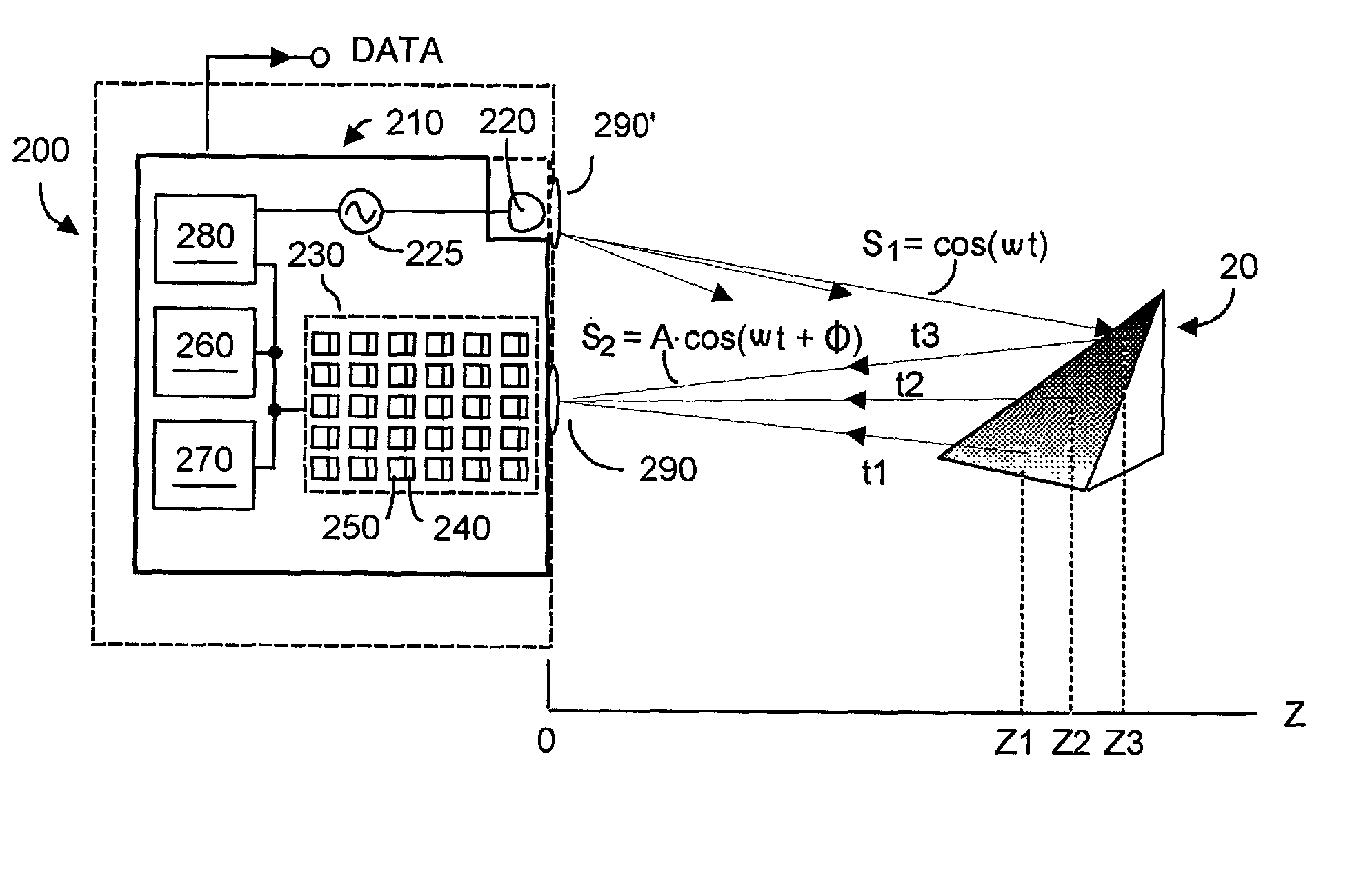
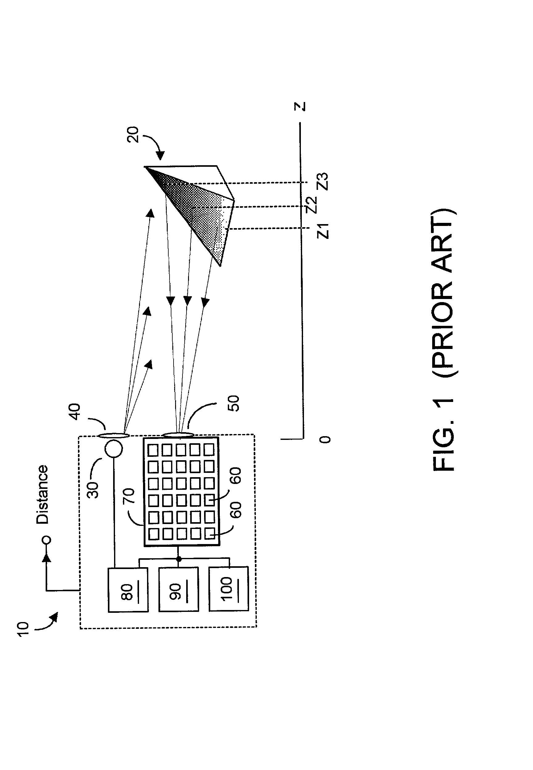
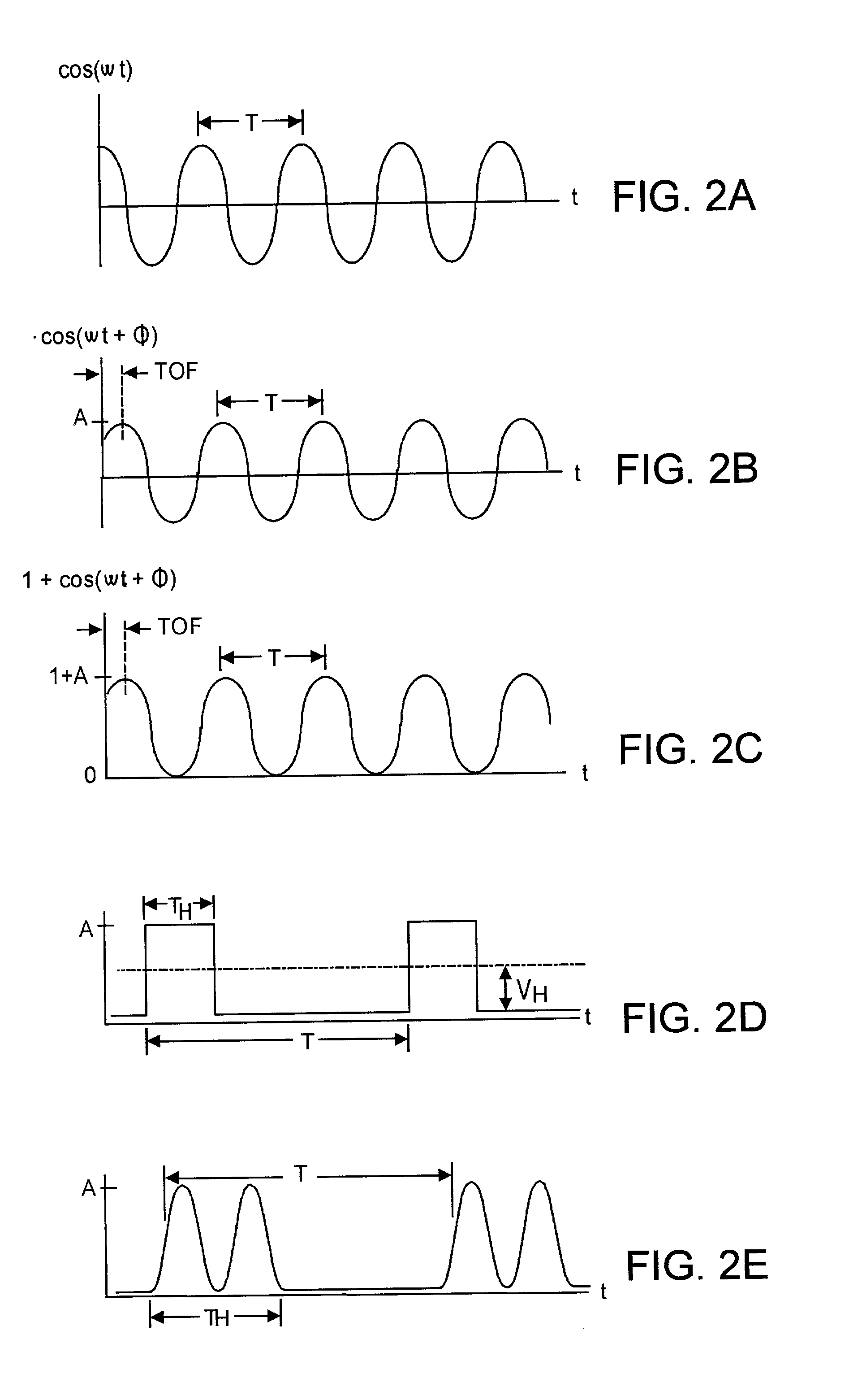
[0057] The present invention advantageously transmits and detects optical energy that is periodic with a high frequency component, and relies upon phase shift between transmitted and detected waveforms to discern time-of-flight and thus z-distance data. Although pulsed-type periodic waveforms may be used, the present invention will be described with respect to the emission and detection of sinusoidal waveforms, as such waveforms are rather easily analyzed mathematically. However it is to be understood that periodic pulsed waveforms with a high frequency component including imperfect sinusoidal waveforms are representable mathematically as groupings of perfect sinusoidal waveforms of varying coefficients and frequency multiples. The transmission and detection of such waveforms can advantageously permit use of relatively inexpensive low peak-power optical emitters, and the use of relatively lower bandwidth amplifiers. This is in contrast to applicant's referenced U.S. Pat. No. 6,323,9...


PUM


Abstract

A preferably CMOS-implementable system measures distance and/or brightness by illuminating a target with emitted optical energy having a modulated periodic waveform whose high frequency component may be idealized as S.sub.1=cos(.omega..multidot.t). A fraction of the emitted optical energy is reflected by a target and detected with at least one in a plurality of semiconductor photodetectors. Photodetector quantum efficiency is modulated to process detected signals to yield data proportional to the distance z separating the target and photodetector. Detection includes measuring phase change between the emitted optical energy and the reflected fraction thereof. Quantum efficiency can be modulated with fixed or variable phase methods and may be enhanced using enhanced photocharge collection, differential modulation, and spatial and temporal multiplexing. System power requirements may be reduced with inductors that resonate with photodetector capacitance at the operating frequency. The system includes on-chip photodetectors, associated electronics, and processing.

Description

RELATION TO PREVIOUSLY FILED APPLICATIONS[0001] Priority is claimed from applicants' co-pending U.S. provisional patent application Ser. No. 60 / 254,873 filed on Dec. 11, 2000 entitled "CMOS 3D Multi-Pixel Sensor Using Photodiode Quantum Efficiency Modulation". Applicants incorporate said application herein by reference. Applicants also refer to and incorporates by reference herein co-pending U.S. utility application Ser. No. 09 / 876,373 filed Jun. 6, 2001 entitled "CMOS-Compatible Three-Dimensional Image Sensing Using Reduced Peak Energy".FIELD OF THE INVENTION[0002] The invention relates generally to range finder type image sensors, especially range finder image sensors that are implementable on a single integrated circuit using CMOS fabrication, and more particularly to reducing power consumption of systems utilizing such sensors.BACKGROUND OF THE INVENTION[0003] Electronic circuits that provide a measure of distance from the circuit to an object are known in the art, and may be ex...

Claims


Application Information

Patent Timeline
IPC IPC(8): G01S7/4914G01S17/36G01S17/894
CPCG01S17/36G01S17/89G01S7/4914G01S17/894
Inventor BAMJI, CYRUSCHARBON, EDOARDO
Owner MICROSOFT TECH LICENSING LLC
Why Eureka
Try Eureka