Ultraviolet-transparent conductive film and process for producing the same

Inactive Publication Date: 2003-06-12
HOYA CORP +1
View PDF2 Cites 48 Cited by
  • Summary
  • Abstract
  • Description
  • Claims
  • Application Information

AI Technical Summary

Benefits of technology

0055] An YSZ single-crystal substrate was installed in a laser-ablation ultra-high vacuum chamber (St-1200 G made by IRIE KOKEN CO., LTD). Then, the substrate is heated by an IR lamp heater, and oxygen gas having a p

Problems solved by technology

These materials have a bandgap of about 3.2 eV or its equivalent wavelength of about 390 nm, and thereby does not allow transmission of near-ultraviolet light or deep-ultraviolet light having a wavelength shorter than the equivalent wavelength.
However, there has not been provided any report of verifying transparent conductivity in a thin-film form required for applications to transparent electrodes or antistatic films.
Further, this report describes neither transparency nor applicability to transparent conductive films.
However, the conductive property was verified only at a surface layer having a depth of about 50 .mu.m from the surface of the single crystal, and the inside of the single crystal was still insulative.
However, there is no prior art disclosing a ZnGa.sub.2O.sub.4 thin-film having transparent conductivity.
However, neither the ITO nor the ATO allows sufficient transmission of a blue light having a wavelength of about 400 nm and an ultraviolet light having a wavelength shorter than the blue light.
Thus, if the thickness of the transparent electrode is increased, the light-emitting devices will have a significantly reduced light-emitting efficiency.
In addition, the solar cells cannot pick up any ultraviolet light from sunlight.
Further, no antistatic film allowing transmission of ultraviolet light has been developed.
However, there has not been developed any ultraviolet-transparent conductive film usable for this purpos

Method used


Image

  • Ultraviolet-transparent conductive film and process for producing the same
  • Ultraviolet-transparent conductive film and process for producing the same

Examples


example 4

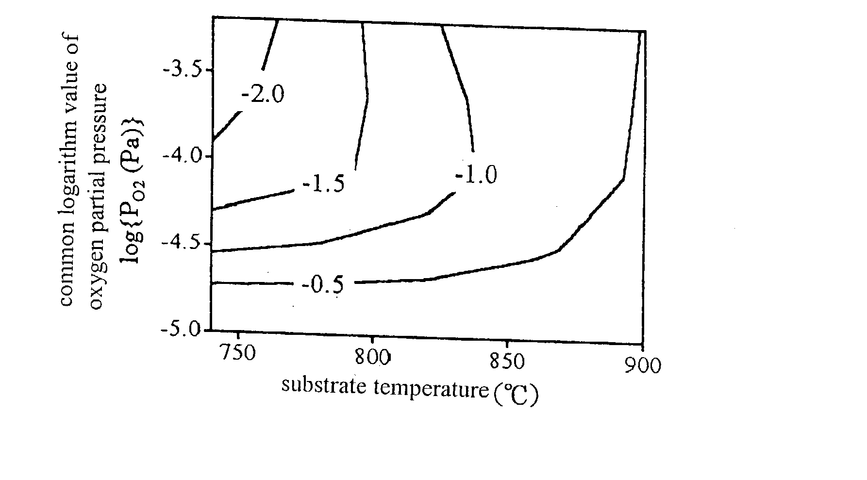
[0058] A silica glass substrate was installed in the laser-ablation ultra-high vacuum chamber. Then, the substrate is heated in the range of 700 to 900.degree. C. by the IR lamp heater, and oxygen gas having a partial pressure in the range of 1.times.10.sup.-5 to 1.times.10.sup.-3 Pa was introduced into the chamber. A high-purity Ga.sub.2O.sub.3 containing 1 mol % of SnO.sub.2 as a dopant was used as a target, and Ga.sub.2O.sub.3 was deposited on the silica glass substrate opposed to the target at a distance of 30 mm by irradiating the target with the ArF excimer laser beam. A resulting film has a thickness of about 100 nm.

[0059] A conductivity of the thin film with respect to the substrate temperature and oxygen partial pressure is shown in FIG. 1 as a contour diagram. The horizontal axis, vertical axis and contour indicate the substrate temperature, the common logarithm value of the oxygen partial pressure and the common logarithm value of the conductivity, respectively. At a subs...

example 5

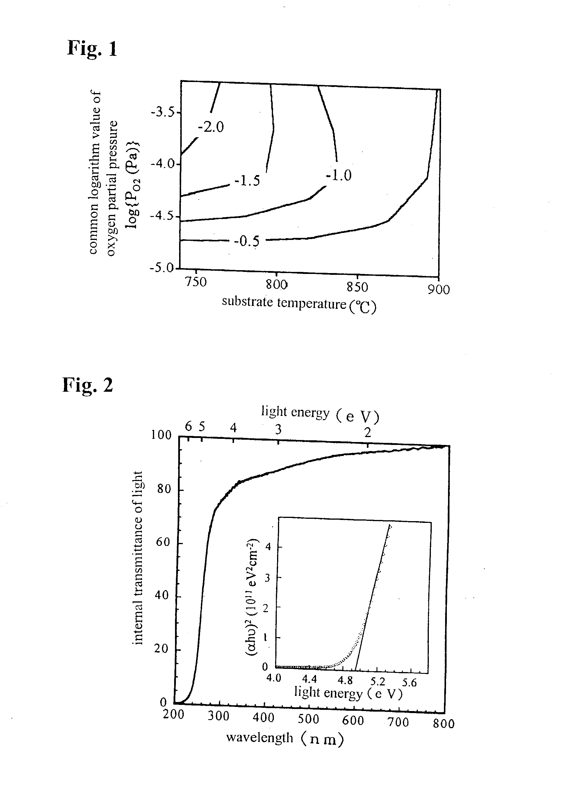
[0060] As in Example 4, Ga.sub.2O.sub.3 was deposited on a silica glass substrate. Under the conditions with a substrate temperature of 880.degree. C. and an oxygen partial pressure of 6.times.10.sup.-5 Pa, a .beta.-Ga.sub.2O.sub.3 thin-film having a conductivity of 1.0 S / cm was obtained. This thin film has a mobility of 0.44 cm.sup.2 / Vs and a carrier density of 1.4.times.10.sup.19 / cm.sup.3. A light transmittance spectrum of the thin film is shown in FIG. 2. The horizontal and vertical axes indicate the wavelength of light and the internal transmittance (int) of light, respectively.

[0061] The term "internal transmittance" means a light transmittance in which the contribution of the light reflection on the surface of the thin film is removed therefrom; or a value calculated based on the formula T (int)=T (obs) / (100-R (obs)) using a light transmittance T (obs) and a reflectance R (obs) measured by the ultraviolet / visible spectrophotometer; or a percentage ratio of a transmitted light ...


PUM

PropertyMeasurementUnit
Temperatureaaaaaaaaaa
Fractionaaaaaaaaaa
Fractionaaaaaaaaaa

Abstract

The present invention provides an ultraviolet-transparent conductive film comprising a Ga2O3 crystal. The film has a transparency in the wavelength range of 240 to 800 nm, or 240 to 400 nm, and an electric conductivity induced by an oxygen deficiency or dopant in the Ga2O3 crystal. The dopant includes at least one element selected from the group consisting of the Sn, Ge, Si, Ti, Zr, Hf, V, Nb, Ta, Cr, Mo and W. The ultraviolet-transparent conductive film is formed through either one of a pulsed-laser deposition method, sputtering method, CVD method and MBE method, under the conditions with a substrate temperature of 600 to 1500° C. and an oxygen partial pressure of 0 to 1 Pa.

Description

[0001] The present invention relates to an ultraviolet-transparent conductive layer having a transparency in the wavelength range of the ultraviolet to visible region and therefore providing applicability to a transparent electrode or ultraviolet-transparent antistatic film for light-emitting devices or solar cells.[0002] Heretofore, a transparent conductive film has been used as a transparent electrode for solar cells or flat panel displays. For these purposes, the transparent conductive film has been typically made of tin-doped iridium oxide (ITO), fluorine-doped tin oxide (FTO) or aluminum-doped zinc oxide (AZO), with particular emphasis on the transparency in the visible region of 400 to 800 nm. As another example, there have also been known non-crystalline transparent conductive films represented by Ga.sub.2O.sub.3 (Japanese Patent Laid-Open Publication No. 7-335030), Ga.sub.2O.sub.2--In.sub.2O.sub.2 (Japanese Patent Laid-Open Publication No. 9-259640), and AB.sub.2-xO.sub.4-y ...

Claims


Application Information

Patent Timeline
IPC IPC(8): C23C14/08C23C16/40C30B23/02C30B25/02H01B5/14H01B13/00H01L31/0224H01L31/04H01L31/18H01L51/00H01L51/40
CPCC23C14/08C23C16/40H01L2924/0002Y02E10/50H01L51/0021H01L33/42H01L31/1884C30B23/02C30B25/02H01L31/022466C30B29/16H01L2924/00H10K71/60
Inventor OTA, HIROMICHIORITA, MASAHIROHOSONO, HIDEOHIRANO, MASAHIRO
Owner HOYA CORP
Why Eureka
Try Eureka