

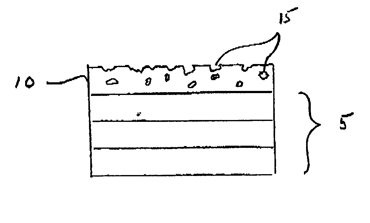
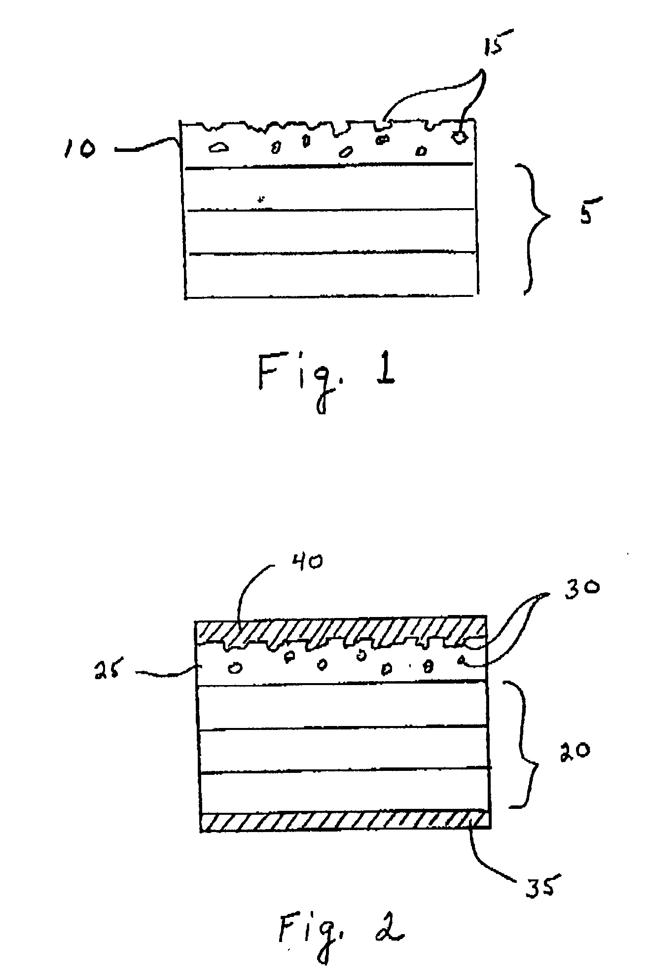
Dielectric structure
a dielectric structure and dielectric material technology, applied in the direction of dielectric characteristics, feed-through capacitors, fixed capacitor details, etc., can solve the problems of limiting the space available for the mounting of active components, such as integrated circuits, and the capacitance fails to adequately address the need for embedded capacitors, and achieves increased surface area of capacitor dielectric materials, improved adhesion of plated electrodes, and improved adhesion
- Summary
- Abstract
- Description
- Claims
- Application Information
AI Technical Summary
Benefits of technology
Problems solved by technology
Method used
Image

Examples
example 1
[0062] Barium acetate, Ba(CH.sub.3COO).sub.2, (1 mol) is dissolved in a mixed solution of 20 mol ethanol, 25 mol acetic acid, and 1 mol glycerol, and then the solution is stirred for 2 hr. After stirring, 1 mol of Ti[O(CH.sub.2).sub.3CH.sub.3].sub.4 is added to the solution, followed by stirring for another 2 hr to prepare a barium titanate sol.
[0063] A sample of this sol is spin coated on a conductive substrate at 2000 rpm for 45 sec. After the solution is spin coated, the sample is heated at 170.degree. C. for 1 hr in a nitrogen-gas atmosphere, followed by two steps of successive annealing of 400.degree. C. for 1 hr and 700.degree. C. for 1 hr in air. The thickness of the annealed dielectric sample prepared using this procedure is .about.100 nm.
[0064] To another sample of the sol is added cross-linked polymeric porogen particles. The porogen particles are added in an amount sufficient to provide 40% porogen by weight, based on the total weight of the sol. The porogen particles con...
example 2
[0065] The textured surface of the dielectric structure of Example 1 is catalyzed and subjected to an electroless nickel plating bath to deposit a layer of nickel on the textured surface. The nickel plated dielectric is next subjected to a nickel electroplating bath to increase the thickness of the nickel deposit.
example 3
[0066] The procedure of Example 2 is repeated except that the electrolessly nickel plated dielectric is subjected to a copper electroplating bath to deposit a layer of copper on the electroless nickel layer.
PUM
| Property | Measurement | Unit |
|---|---|---|
| Fraction | aaaaa | aaaaa |
| Particle size | aaaaa | aaaaa |
| Thickness | aaaaa | aaaaa |
Abstract
Description
Claims
Application Information