Light emitting device

a technology of light-emitting devices and light-emitting tubes, which is applied in the direction of electroluminescent light sources, sustainable manufacturing/processing, and final product manufacturing, etc., can solve the problems of affecting the utilization rate of electroluminescence, and posing a small angle of view

Inactive Publication Date: 2003-08-07
SEMICON ENERGY LAB CO LTD
View PDF1 Cites 101 Cited by
  • Summary
  • Abstract
  • Description
  • Claims
  • Application Information

AI Technical Summary

Benefits of technology

[0134] As explained above, the concentration of oxygen as an impurity element in layers made from organic compounds that function as hole injecting layers, hole transporting layers, light emitting layers, and the like in organic light emitting elements can be reduced to a level equal to or less than 5.times.10.sup.19 / cm, preferably equal to or less than 1.times.10.sup.19 / cm.sup.3, by using the present invention. Further, semiconductor films, gate insulating films, and gate electrodes, which are the main structural elements of TFTs, are surrounded by inorganic insulating materials selected from the group consisting of silicon nitride, silicon oxynitride, aluminum oxynitride, aluminum oxide, and aluminum nitride with the present invention, thus providing a structure in which contamination by alkaline metals and organics is prevented. On the other hand, organic light emitting elements contain alkaline metals, and a structure in which penetration of oxygen and moisture from the outside is prevented by surrounding the organic light emitting elements using an inorganic insulating material selected from the group consisting of silicon nitride, silicon oxynitride, aluminum oxynitride, aluminum oxide, aluminum nitride, DLC, and carbon nitride is achieved. In accordance with this type of structure, a light emitting device in which elements having different characteristics with respect to impurities are combined, without mutual interference, can thus be completed.

Problems solved by technology

Liquid crystal display devices are employed as image displaying means in various types of electronic devices, but have a structural disadvantage in that they possess a small angle of view.
However, problems remain in that degradation phenomena exist, and this impedes utilization of electroluminescence.
However, whichever type is used, organic compounds made purely from only basic structural units are rare, and there are also times when dissimilar bonds and impurities are mixed in during manufacturing processes, and times when various additives such as pigments are added.
Further, there are materials which deteriorate due to moisture, materials which easily oxidize, and the like among these materials.
Impurities form localized levels within a forbidden band caused by oxygen in semiconductor elements having semiconductor junctions such as diodes, and the localized levels become a factor in junction leakage and reducing the carrier lifetime, and are known to greatly lower the characteristics of the semiconductor elements.
Melting occurs if the melting point, or the glass transition temperature, of the organic compound is low, and electric fields concentrate in portions where pinholes or cracks exist, causing dielectric breakdown.
Regarding the factor (5), all organic compounds used in the organic light emitting elements are amorphous materials, and crystallize due to heat emission when stored over a long period of time or are aged, and it can be thought that almost none are capable of stably preserving their amorphous structure.
Further, irregularities such as film cracking and fracture due to distortion generated by a difference in the thermal expansion coefficient of structural materials leads to the factor (6).
In addition, progressive irregularities such as dark spots also are generated in those portions.
Dark spots are suppressed considerably by raising the level of a sealing technique used, but actual degradation is generated by a combination of the aforementioned factors, and it is difficult to prevent.
As a result, it is expected that the electron transporting characteristics become deteriorated.
On the other hand, TFTs using a semiconductor as an active layer are damaged by alkaline metals and alkaline earth metals, which are used as cathode materials in organic light emitting elements.
That is, mobile ions in these materials get mixed into a gate insulating film or within an active layer, and switching operations thus become impossible.
However, these types of organic resin materials are hygroscopic.

Method used


Image

  • Light emitting device
  • Light emitting device
  • Light emitting device

Examples


Embodiment Construction

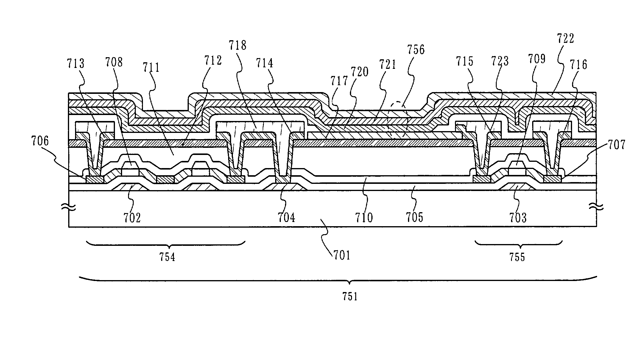
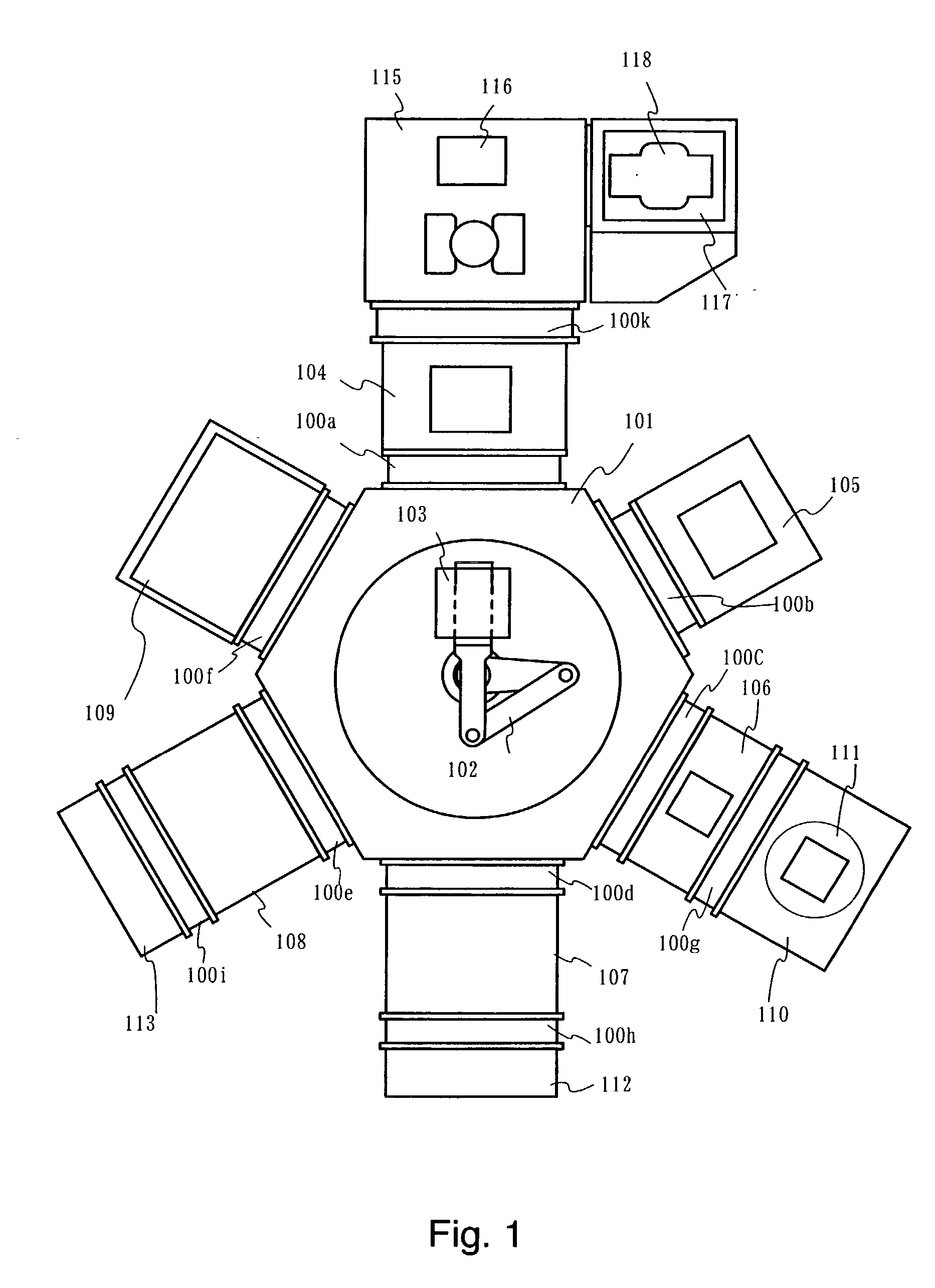
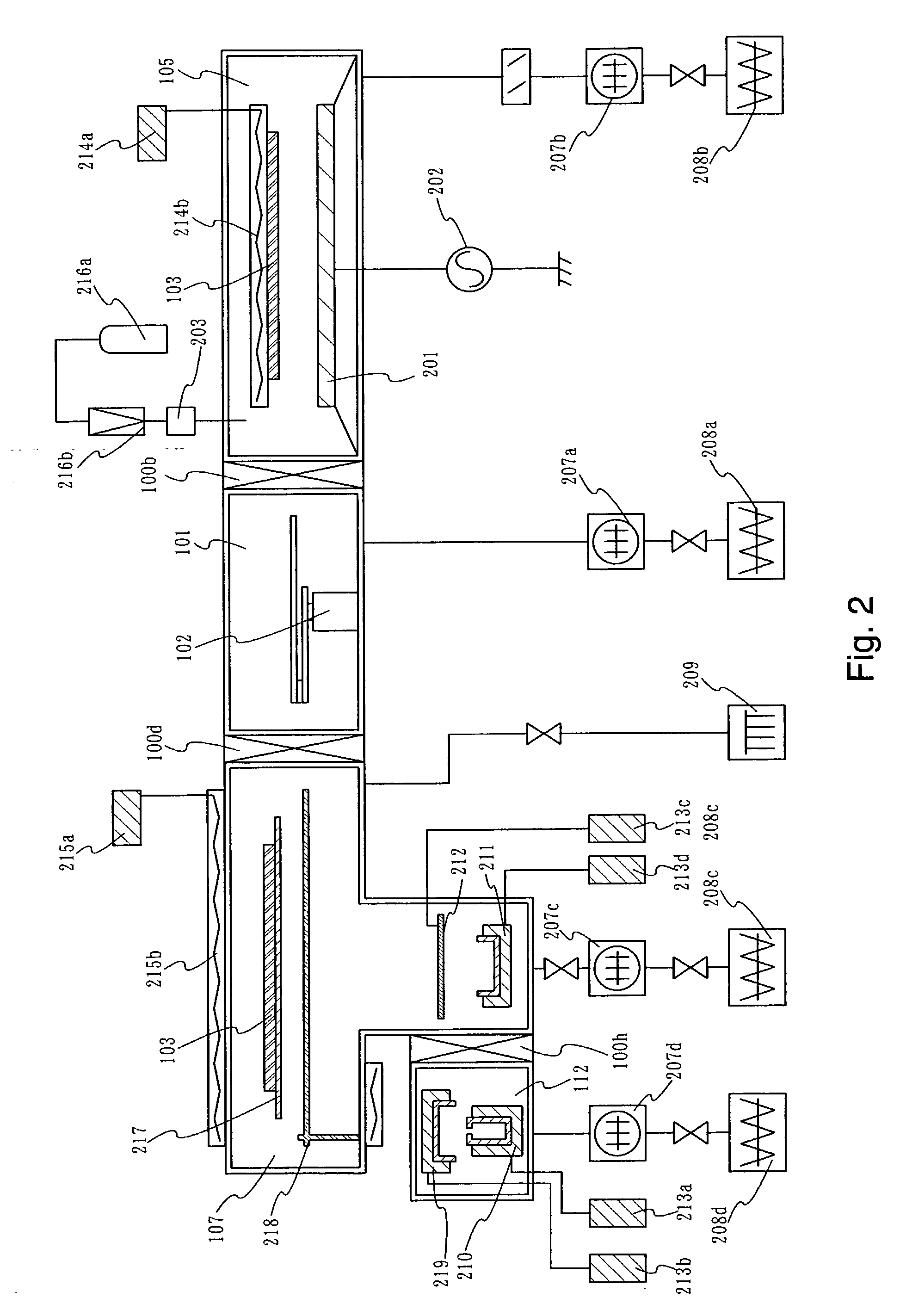
[0063] An example of an apparatus for manufacturing a light emitting device capable of reducing the concentration of impurities contained in organic compounds, such as oxygen and moisture, is explained using FIG. 1. FIG. 1 shows an apparatus for performing film formation and sealing of layers made from organic compounds and a cathode. A conveyor chamber 101 is coupled to a loading chamber 104, a preprocessing chamber 105, an intermediate chamber 106, a film formation chamber(A) 107, a film formation chamber (B) 108, and a film formation chamber (C) 109 through gates 100a to 100f. The preprocessing chamber 105 is provided with the aim of dehydrogenation of processing substrates, degasification processing, and improving surface quality, and heat treatment processing within a vacuum or plasma processing using an inert gas becomes possible.

[0064] The film formation chamber (A) 107 is a processing chamber mainly for forming a film made from a low molecular weight organic compound by evap...


PUM

PropertyMeasurementUnit
speedaaaaaaaaaa
work functionaaaaaaaaaa
quantum efficiencyaaaaaaaaaa

Abstract

An objective is to increase the reliability of a light emitting device structured by combining TFTs and organic light emitting elements. A TFT (1201) and an organic light emitting element (1202) are formed on the same substrate (1203) as structuring elements of a light emitting device (1200). A first insulating film (1205) which functions as a blocking layer is formed on the substrate (1203) side of the TFT (1201), and a second insulating film (1206) is formed on the opposite upper layer side as a protective film. In addition, a third insulating film (1207) which functions as a barrier film is formed on the lower layer side of the organic light emitting element (1202). The third insulating film (1207) is formed by an inorganic insulating film such as a silicon nitride film, a silicon oxynitride film, an aluminum nitride film, an aluminum oxide film, or an aluminum oxynitride film. A fourth insulating film (1208) and a partitioning layer (1209) formed on the upper layer side of the organic light emitting element (1202) are formed using similar inorganic insulating films.

Description

[0001] 1. Field of the Invention[0002] The present invention relates to a light emitting device prepared with a light emitting element capable of obtaining fluorescence or phosphorescence. In particular, the present invention relates to a light emitting device in which an active element such as an insulated gate transistor or a thin film transistor, and a light emitting element connected to the active element, are formed in each pixel.[0003] 2. Description of the Related Art[0004] Display devices using liquid crystals are structures that typically employ a back light or a front light, and display an image by using light from the back light or the front light. Liquid crystal display devices are employed as image displaying means in various types of electronic devices, but have a structural disadvantage in that they possess a small angle of view. In contrast, the angle of view is wide for display devices that use a light emitter capable of obtaining electroluminescence as displaying m...

Claims


Application Information

Patent Timeline
Patent Type & Authority Applications(United States)
IPC IPC(8): H05B33/22H01L27/32H01L51/52
CPCH01L27/3246H01L27/3258H01L51/5253H01L51/56H01L2227/323H01L51/5088H01L27/3244H01L51/0035H01L51/0036H01L51/5056H01L51/5237Y02E10/549Y02P70/50H10K59/123H10K59/122H10K59/124H10K85/111H10K85/113H10K50/844H10K50/84H10K59/1201H10K71/00H05B33/22H10K50/11H10K50/15H10K50/17H10K50/846H10K50/8426H10K59/12H10K77/111H10K85/10H10K85/311H10K85/324H10K85/342H10K85/626H10K85/631H10K85/633H10K85/6572H10K2101/10H10K2102/00H10K2102/311H10K2102/351
Inventor YAMAZAKI, SHUNPEITAKAYAMA, TORU
Owner SEMICON ENERGY LAB CO LTD
Why Eureka
Try Eureka