Method for producing nitride semiconductor crystal, and nitride semiconductor wafer and nitride semiconductor device

a technology of nitride semiconductor and semiconductor wafer, which is applied in the direction of polycrystalline material growth, crystal growth process, chemically reactive gas, etc., can solve the problems of high cost, high cost, and extremely poor stability of devices using high-dislocation-density semiconductors

Inactive Publication Date: 2003-10-02
SUMITOMO CHEM CO LTD
View PDF9 Cites 55 Cited by
  • Summary
  • Abstract
  • Description
  • Claims
  • Application Information

AI Technical Summary

Benefits of technology

0007] Accordingly, an object of the present invention is to provide a method for producing a nitride semiconductor crystal having a small dislocation density on the entire surface of a substrate by properly controlling its crystal growth, a nitride semiconductor wafer having the nitride semiconductor crystal obtained by such method, and a nitride semiconductor device formed with such a nitride semiconductor wafer.

Problems solved by technology

However, because the single crystal substrate is not only technically difficult to obtain but also high in cost, a semiconductor crystal different from the substrate should often be caused to grow on the substrate.
However, when a semiconductor different from a substrate is caused to grow on the substrate, dislocations are likely introduced in a high density into a grown semiconductor epitaxial layer, because of the mismatch of various characteristics such as lattice, a thermal expansion coefficient, surface energy, etc.
Because the dislocations in the semiconductors may constitute non-radiative recombination centers, scattering centers, etc. in semiconductor devices such as optical devices, electronic devices, etc., devices using high-dislocation-density semiconductors are extremely poor in characteristics and stability.
Because bulk crystal growth is also difficult in nitride semiconductors typically including gallium nitride (GaN), aluminum gallium nitride (AlGaN), indium gallium nitride (InGaN), etc., single crystal substrates with practically acceptable sizes have not been obtained yet.
Still, dislocations remain serious problems as described above.
However, the reduction of a dislocation density by the two-stage growing method is still insufficient, and the dislocation density often cannot be reduced sufficiently depending on the types and structures of a crystal-growing apparatus.
Even in such a case, the apparatuses may be subjected to variations in conditions, etc. for a long period of operation, affecting crystal growth conditions.
Therefore, it is difficult to stably grow nitride semiconductor layers with small dislocation densities.

Method used


Image

  • Method for producing nitride semiconductor crystal, and nitride semiconductor wafer and nitride semiconductor device
  • Method for producing nitride semiconductor crystal, and nitride semiconductor wafer and nitride semiconductor device
  • Method for producing nitride semiconductor crystal, and nitride semiconductor wafer and nitride semiconductor device

Examples


example 2

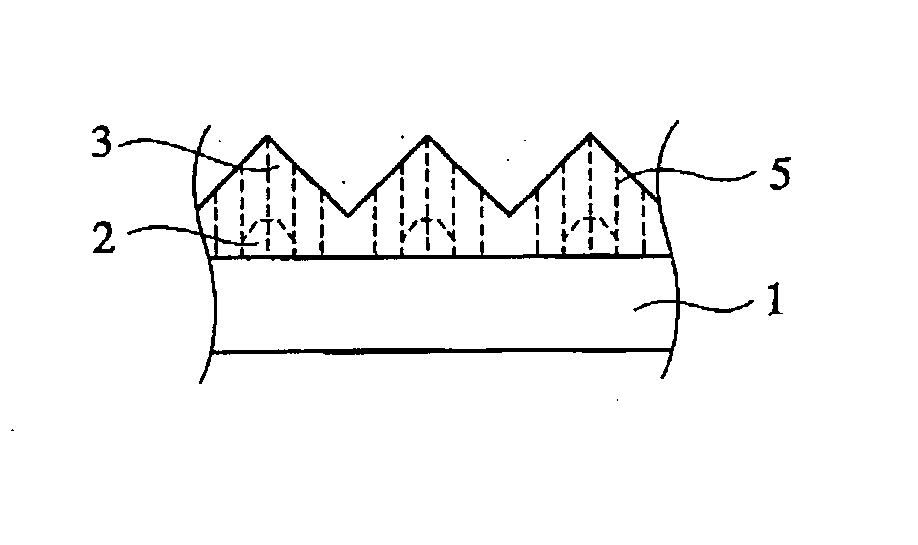
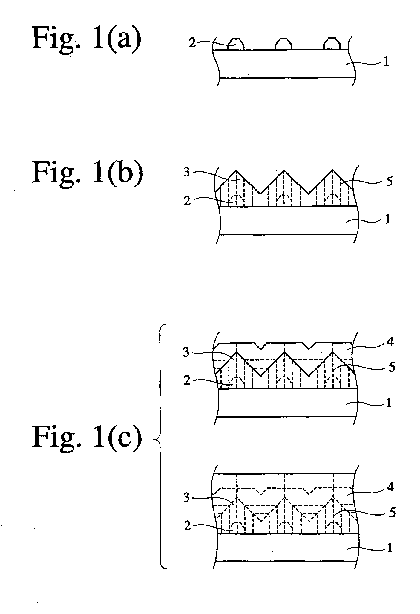
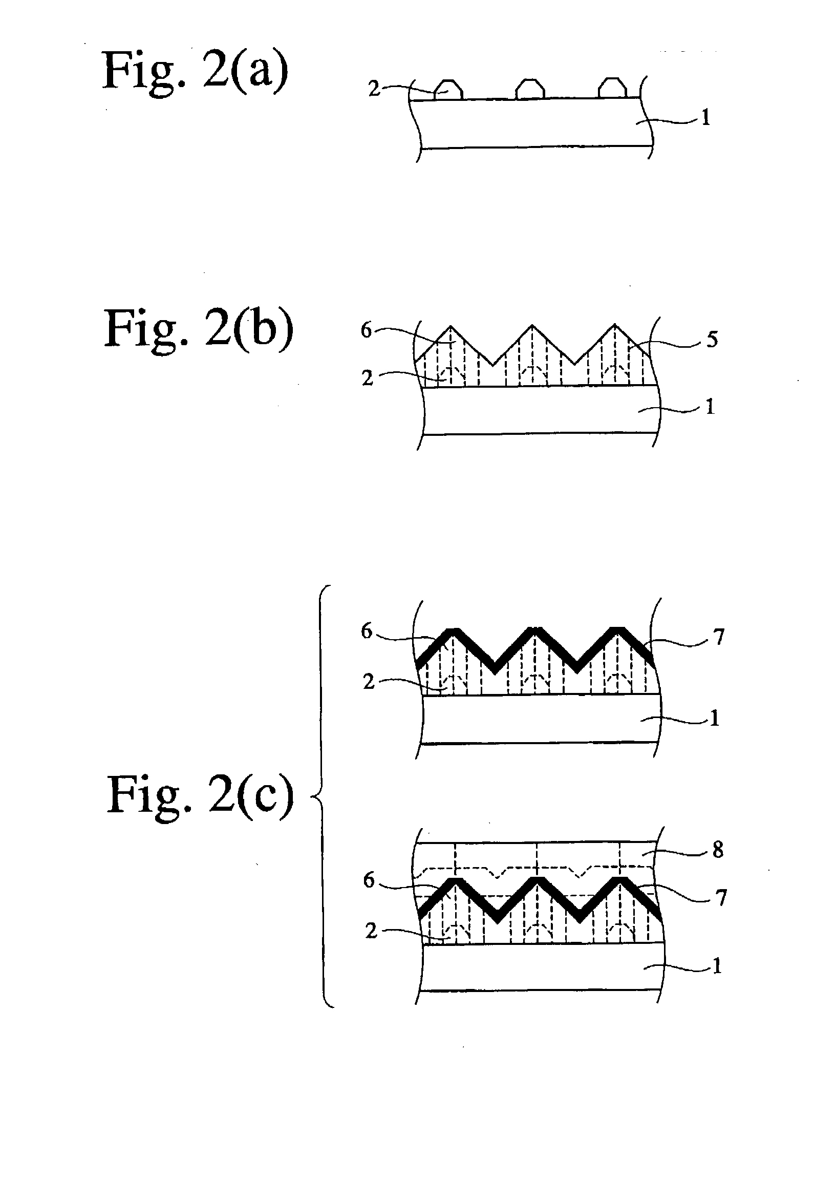
[0078] Investigation was conducted on the relation between a hydrogen concentration in the crystal-growing atmosphere and a dislocation density in the step (b). A nitride semiconductor crystal was caused to grow on the substrate, and the dislocation density on a surface of the resultant nitride semiconductor crystal layer was investigated, in the same manner as in Example 1 except for changing a ratio of an H.sub.2 gas to an N.sub.2 gas in the carrier gas, and setting a crystal-growing temperature Tg.sub.2 at 900 C in the step (b). At this time, with the total flow rate of the carrier gas (80 slm) kept constant, the concentration of an H.sub.2 gas was changed in a range of 0-100%. FIG. 7 is a graph showing the relation between the hydrogen concentration in the atmosphere and a dislocation density. As is clear from FIG. 7, as the hydrogen concentration increased, the dislocation density decreased, and when the hydrogen concentration was 100%, the dislocation density was 5.2.times.10....

example 3

[0079] Investigation was conducted on the relation between the crystal-growing temperature Tg.sub.3 and a dislocation density in the step (c). A nitride semiconductor crystal was caused to grow on the substrate, and the dislocation density on the surface of the resultant nitride semiconductor crystal layer was investigated, in the same manner as in Example 2 except for changing Tg.sub.3, and setting the hydrogen concentration in the crystal-growing atmosphere at 100% in the step (b). FIG. 8 is a graph showing the relation between the crystal-growing temperature Tg.sub.3 and a dislocation density. As is clear from FIG. 8, as the Tg.sub.3 increased, the dislocation density decreased, and the dislocation density was 3.8.times.10.sup.8 cm.sup.-2 at Tg.sub.3 of 1120 C. This appears to be due to the fact that the higher the growing temperature of the nitride semiconductor crystal layer in the step (c), the more the growth in a lateral direction was accelerated, exerting larger effect on c...

example 4

[0080] Investigation was conducted on the relation between the crystal-growing atmosphere pressure in the step (c) and a dislocation density. A nitride semiconductor crystal was caused to grow on the substrate, and the dislocation density on the surface of the resultant nitride semiconductor crystal layer was investigated, in the same manner as in Example 3 except for changing the flow rate of the carrier gas by changing the atmosphere pressure in the growing apparatus, and setting the crystal-growing temperature Tg.sub.3 at 1120 C in the step (c). FIG. 9 is a graph showing the relation between the crystal-growing atmosphere pressure in the step (c) and a dislocation density. As is clear from FIG. 9, the dislocation density decreased with the reduction of an atmosphere pressure, and the dislocation density was 3.times.10.sup.8 cm.sup.-2 at an atmosphere pressure of 76 Torr. It is presumed that the lower the atmosphere pressure in the step (c), the more the growth in a lateral direct...


PUM

PropertyMeasurementUnit
temperatureaaaaaaaaaa

Abstract

A method for producing a nitride semiconductor crystal comprising a step (a) for forming fine crystal particles made of a nitride semiconductor on a substrate; a step (b) for forming a nitride semiconductor island structure having a plurality of facets inclined relative to a surface of the substrate with the fine crystal particles as nuclei; and a step (c) for causing the nitride semiconductor island structure to grow in a direction parallel with a surface of the substrate to merge a plurality of the nitride semiconductor island structures with each other, thereby forming a nitride semiconductor crystal layer having a flat surface; the steps (a)-(c) being continuously conducted in the same growing apparatus.

Description

[0001] The present invention relates to a method for producing a nitride semiconductor crystal having a small dislocation density, a nitride semiconductor wafer having a nitride semiconductor crystal formed by such a method, and a nitride semiconductor device produced therefrom.[0002] The easiest method for forming a semiconductor epitaxial layer is generally to form a single crystal substrate made of the same material as that of a semiconductor to be. grown, and to cause a vapor-phase growth of a semiconductor crystal on the resultant substrate, with actual success in various materials. However, because the single crystal substrate is not only technically difficult to obtain but also high in cost, a semiconductor crystal different from the substrate should often be caused to grow on the substrate. In such a case, known combinations of the substrates and the semiconductor crystals are, for instance, GaAs on a silicon substrate, a nitride semiconductor on a sapphire or silicon carbid...

Claims


Application Information

Patent Timeline
Patent Type & Authority Applications(United States)
IPC IPC(8): C30B29/38C30B25/02C30B25/18H01L21/20H01L21/205H01L21/338H01L29/201H01L29/778H01L29/812H01L33/12H01L33/22H01L33/32H01L33/40
CPCC30B25/02C30B29/406C30B29/403C30B25/18
Inventor FUJIKURA, HAJIMEIIZUKA, KAZUYUKI
Owner SUMITOMO CHEM CO LTD
Why Eureka
Try Eureka