Porous power and ground planes for reduced PCB delamination and better reliability

a technology of porous power and ground planes, applied in the field of computer manufacturing, can solve the problems of pcbs being associated with pcbs, pcbs being generally more complex, and many systems today cannot tolerate extended down time necessary, so as to reduce the number of pcbs failures

Inactive Publication Date: 2003-10-23
GLOBALFOUNDRIES INC
View PDF10 Cites 25 Cited by
  • Summary
  • Abstract
  • Description
  • Claims
  • Application Information

AI Technical Summary

Benefits of technology

[0014] Accordingly, the embodiments of the present invention provide power and ground planes that are used in printed circuit boards (PCBs) and that comprise porous, conductive materials. Porous power and ground plane materials allow water and / or other solvents to pass through the power and ground planes, thus decreasing failures in PCBs (or PCBs used as laminate chip carriers) caused by cathodic / anodic filament growth and delamination of insulators. Porous conductive materials may be formed by using metal-coated cloths (such as polyester) or fabrics (such as those made from carbon / graphite or glass fibers), using metal wire mesh instead of metal sheets, using sintered metal, or making metal sheets porous by forming an array of holes in the metal sheets. Metal mesh or fabric may be made in woven or random paper configurations. If an array of holes is formed in a metal sheet, such an array may be formed with no additional processing steps than are performed using conventional methods.
[0027] Since the copper layer formed by the metallizing process is generally too thin to form a suitable electrical bridge between the two layers of the board, copper electroplating is used to deposit a heavy layer of copper in the holes in order to form a suitable copper cross section for carrying current. Copper plating can be followed by tin-lead or tin plating in order to improve solderability.
[0031] Power core 110 in FIG. 6 comprises a dielectric layer 114 sandwiched between two copper layers 112 and 115. Copper layers 112 and 115 may be thicker than copper layers 102 and 104 to provide extra current carrying capability. Power core 110 is a CCL on which no processing has been performed. Copper layer 112 will become the power plane of a PCB, while copper layer 115 will become the ground plane of a PCB (or vice versa). Power core 111 is a representation of power core 110 after power core 110 has been patterned. Power core 111 comprises copper layers 112 and 115 that are now patterned and dielectric layer 114. Copper layer 112 is patterned with two clearance areas 182 and 179, while copper layer 115 is patterned with two clearance areas 184 and 180. These clearance areas will prevent the power and ground planes from contacting PTHs that will be drilled in these locations after power core 111 has been pressed into a composite and holes have been drilled and plated.

Problems solved by technology

Many systems today cannot tolerate the extended down time necessary to replace failed components that make up the computer system.
PCBs are generally more complex, however, and are usually made of conductive, metal power and ground planes and several signal planes containing circuit lines sandwiched between layers of insulator, with metal lines and pads on the top and bottom surface of the sandwich.
There are, however, problems associated with PCBs.
One of the causes of some of these problems is water.
Unfortunately, power and ground planes, which are usually made of copper metal, are not water permeable.
This lack of permeability affects PCBs and can cause failures.
These temperature increases can cause water that has collected at interfaces between the power / ground plane and the insulating layers to flash to steam.
Water increases in volume dramatically as it becomes steam, and this expanding water / steam mixture can cause delamination of the insulator.
In fact, "blisters" can appear in the surface of the insulator, leading to cracking of the insulator, line breakage, package ruptures, cracked PTH barrels, and other similar deleterious effects.
Until water has been removed from the PCB, however, the water can cause blister damage.
These conductive metal dendrites then cause electrical shorts.
Now that PCBs have begun to be used in chip carriers, water migration and the problems associated therewith are more prevalent because there is simply more water in these organic materials.
Therefore, without a way to limit failures caused by cathodic / anodic dendrite growth and delamination of insulators in organic LCCs, PCBs and LCCs will continue to have higher numbers of failures and reliability problems.

Method used


Image

  • Porous power and ground planes for reduced PCB delamination and better reliability
  • Porous power and ground planes for reduced PCB delamination and better reliability
  • Porous power and ground planes for reduced PCB delamination and better reliability

Examples


Embodiment Construction

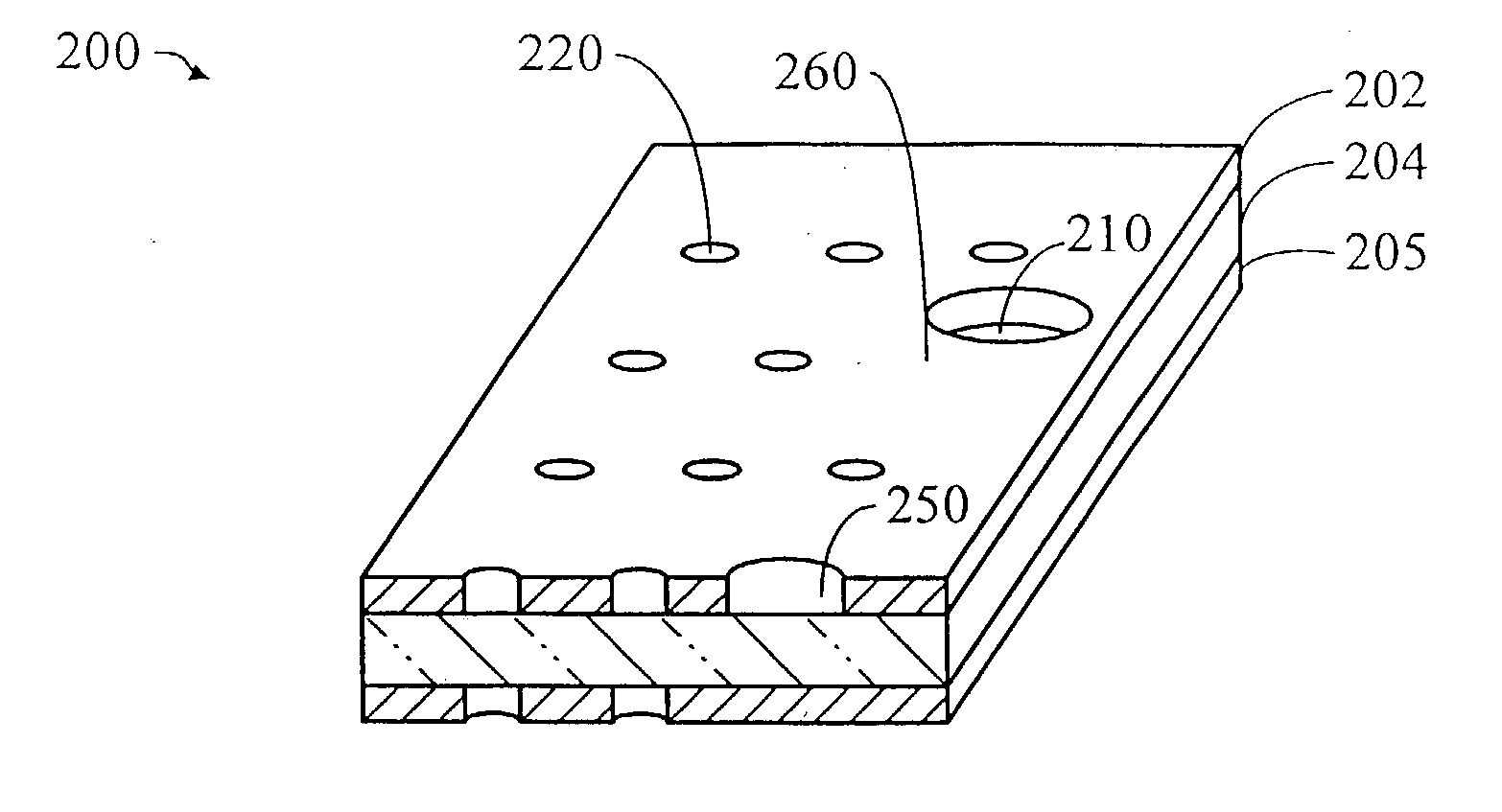
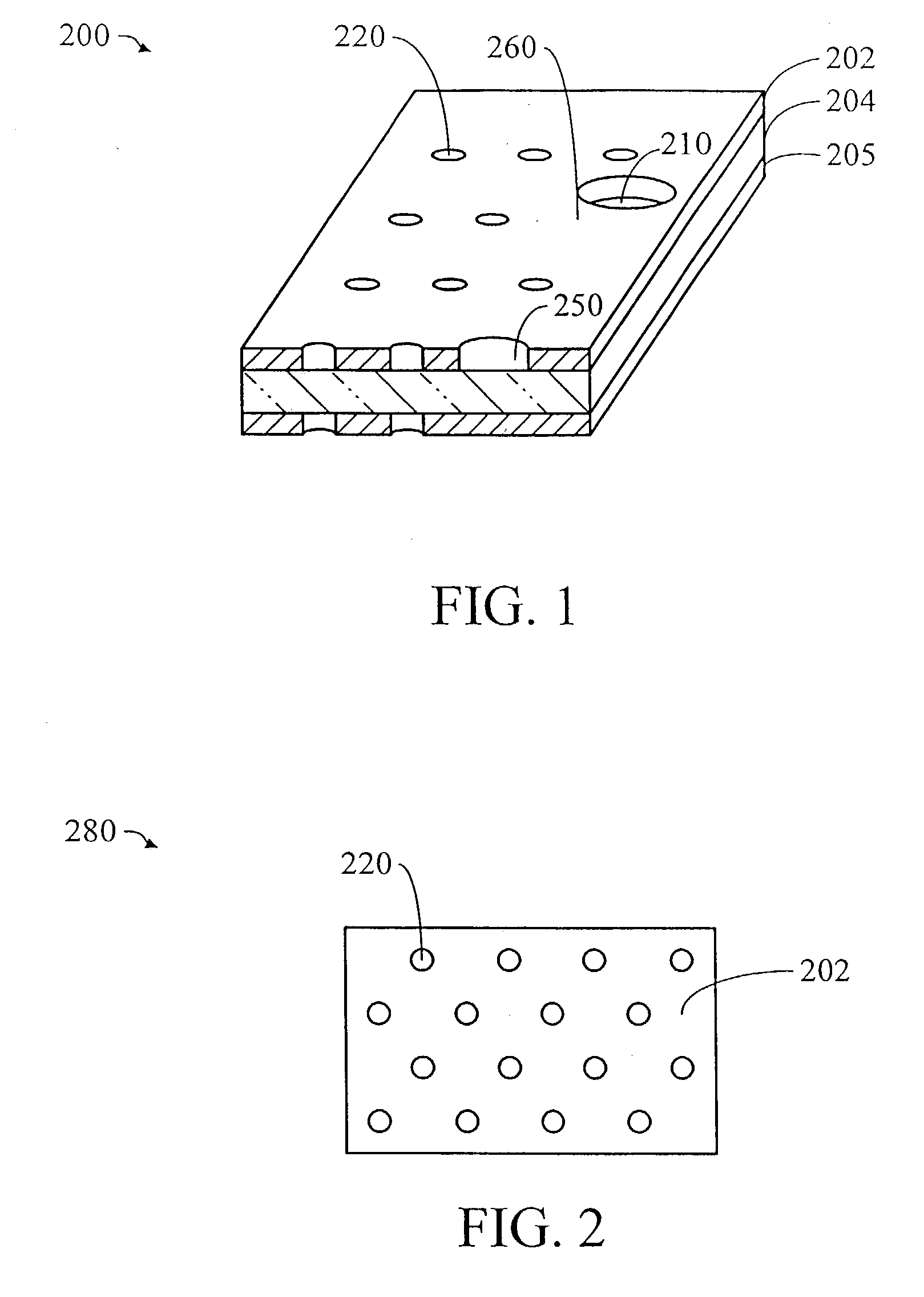
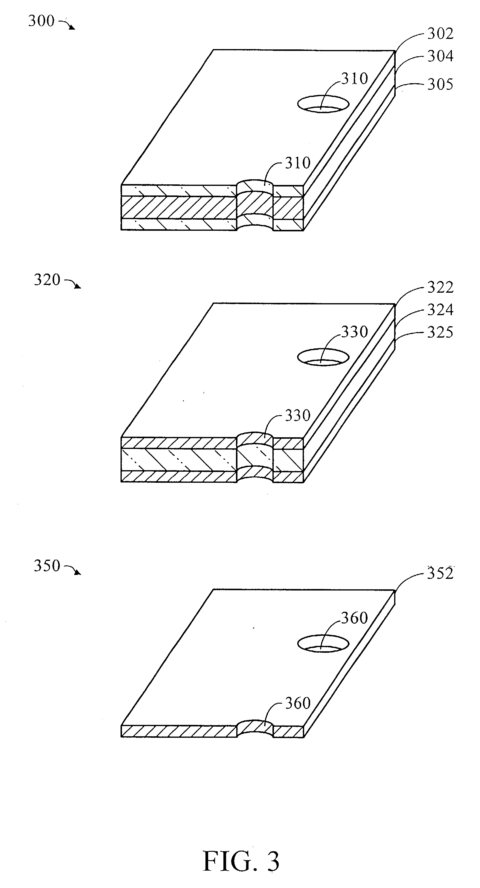
[0036] The preferred embodiments of the present invention overcome the limitations of the prior art by providing power and ground planes that are used in Printed Circuit Boards (PCBs) (or PCBs used as Laminate Chip Carriers (LCCs)) and that contain conductive, porous materials. By providing high porosity, these power and ground plane materials allow water or other solvents to pass through the power / ground planes, thereby reducing or eliminating cathodic / anodic filament (CAF) growth and blisters caused by expanding solvent. Water is the main cause of CAF, but other solvents are known to cause delamination. In particular, trichloroethylene, methylene chloride, benzyl alcohol, and propylene carbonate are solvents that can cause delamination or bubbling effects.

[0037] The preferred embodiments comprise a variety of conductive, porous materials that may be used for the power and ground planes of PCBs. There are a number of materials available that meet the requirement of porous power and...


PUM

PropertyMeasurementUnit
diameteraaaaaaaaaa
diameteraaaaaaaaaa
diameteraaaaaaaaaa

Abstract

Power and ground planes that are used in Printed Circuit Boards (PCBs) and that comprise porous, conductive materials are disclosed. Using porous power and ground plane materials in PCBs allows liquids (e.g., water and / or other solvents) to pass through the power and ground planes, thus decreasing failures in PCBs (or PCBs used as laminate chip carriers) caused by cathodic / anodic filament growth and delamination of insulators. Porous conductive materials suitable for use in PCBs may be formed by using metal-coated organic cloths (such as polyester or liquid crystal polymers) or fabrics (such as those made from carbon / graphite or glass fibers), using metal wire mesh instead of metal sheets, using sintered metal, or making metal sheets porous by forming an array of holes in the metal sheets. Fabrics and mesh may be woven or random. If an array of holes is formed in a metal sheet, such an array may be formed with no additional processing steps than are performed using conventional PCB assembly methods.

Description

[0001] This application is related to a copending patent application by Japp et al., entitled "LOW CTE POWER AND GROUND PLANES", Ser. No. ______, filed ______, and is incorporated herein by reference.[0002] 1. Technical Field[0003] The present invention relates generally to the field of computer manufacturing and more specifically to reducing delamination of, and cathodic / anodic filament growth on, boards used in computers.[0004] 2. Background Art[0005] Computers and similar electronic equipment have become ubiquitous elements in the lives of people. Many businesses, banks, and governments rely on computers for their everyday activities. A large portion of the global community require that computers be reliable, stable facets of their economic, societal, and communication foundations. Computers today are required to run longer, with less down-time, than at any time in the past.[0006] Because computers are so necessary, there has been an increased emphasis by computer designers on re...

Claims


Application Information

Patent Timeline
Patent Type & Authority Applications(United States)
IPC IPC(8): H05K3/38H05K1/02H05K3/42H05K3/46
CPCH05K3/38Y10T29/49126H05K3/4641H05K2201/0116H05K2201/0281H05K2201/029H05K2201/0769H05K2201/09309H05K2201/09681H05K2203/1131Y10S428/901Y10T29/49155Y10T29/49002Y10T428/24917Y10T29/49165Y10T428/24273Y10T156/1052H05K3/429
Inventor JAPP, ROBERT M.POLIKS, MARK D.
Owner GLOBALFOUNDRIES INC
Why Eureka
Try Eureka