Semiconductor device

a technology of semiconductor devices and semiconductors, applied in semiconductor devices, semiconductor/solid-state device details, electrical apparatus, etc., can solve the problems of not having a sufficient effect of lessening the wiring-to-wiring capacitance, the dielectric constant of fluorine-doped silicon oxide films is relatively high, and the wiring delay tends to increas

Inactive Publication Date: 2003-11-20
RENESAS ELECTRONICS CORP
View PDF9 Cites 20 Cited by
  • Summary
  • Abstract
  • Description
  • Claims
  • Application Information

AI Technical Summary

Problems solved by technology

With such progress, the delay coming when signals pass through wirings, i.e., the wiring delay tends to increase.
This is a problem of great proportions in using electronic equipment making use of semiconductor devices.
However, the fluorine-doped silicon oxide film has a relatively high dielectric constant, and can not have a sufficient effect of lessening the wiring-to-wiring capacitance when it is used as the interconnecting insulation layer.
However, in the above related art, the interconnecting insulation layers having the property that the dielectric constant is lower than 3.5 involve a problem that the insulation layers have fundamentally lower mechanical strength such as hardness and elastic modulus than the Silicon oxide film and Silicon nitride film formed by CVD.
In such insulation layers, it has been considered not realistic that the nano-pores are formed in films to make the films into porous films in order to more reduce the dielectric constant, because this may come toward further deterioration of mechanical strength.
Such organic polymers are favorable because their dielectric constant is less than 4, but have disadvantages that they physically have a lower mechanical strength and also higher hygroscopicity and moisture permeability than inorganic films.
When used as interconnecting insulation layers, they may also cause a problem on the reliability of devices, e.g., a lowering of mechanical strength of device structure and corrosion of wirings which is due to absorbed moisture.
However, the size of the nano-pores to be incorporated in the insulation film must be controlled with great care because, if the nano-pores have a large diameter, problems may instead arise such that the mechanical strength as a structure of the insulation film lowers and the leak current flows greatly through the insulation film to lower the breakdown strength that is a characteristic feature as the insulation film.
To deal with silicon wafers made to have larger diameter, a large-size film formation apparatus is required when insulation films are formed by CVD, and it follows that the cost of installation has a great influence on device cost.
This can obstruct any water content which may come from the element surroundings or from the interface between the substrate and the interconnecting insulation layer, permeating through the interior of the interconnecting insulation layer.

Method used


Image

  • Semiconductor device
  • Semiconductor device
  • Semiconductor device

Examples


third example

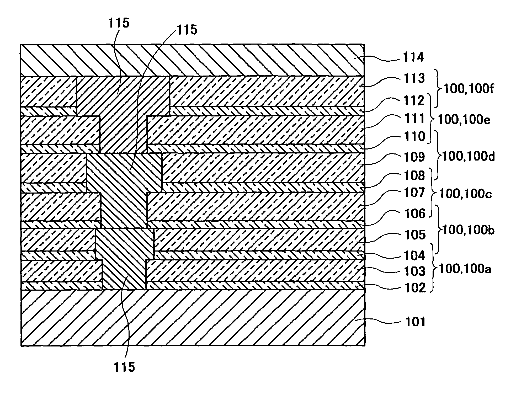
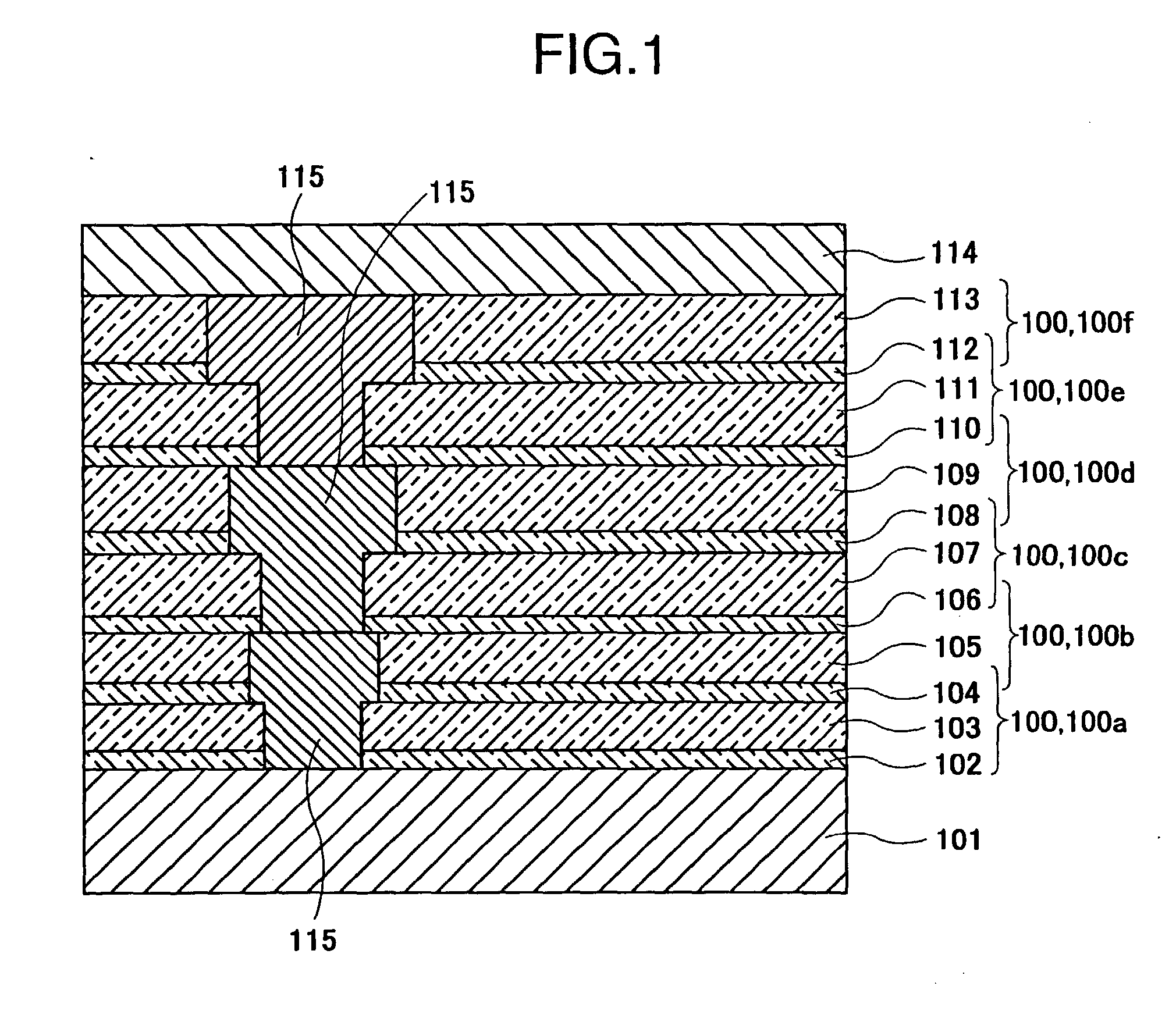
[0069] In this Example, using the same techniques as those in First Example, silicon carbide films were formed by CVD in respect of the insulation layers 102, 104, 106, 108, 110 and 112. Next, the silicon nitride film 114 was formed as the uppermost layer to produce a multi-layer wiring semiconductor device made up of a six-layer Cu wiring 115.

[0070] Thus, a high-performance semiconductor device was obtained the dielectric constant of the whole of interconnecting insulation layers of which was lowered in virtue of the use of, as the etch-stop films or Cu-diffusion barrier films, the silicon carbide films having lower dielectric constant than silicon nitride films.

fourth example

[0071] In this Example, using the same techniques as those in Second Example, silicon carbide films (SiC films) were formed by CVD in respect of the insulation layers 102, 104, 106, 108, 110 and 112. Next, the silicon nitride film 114 was formed as the uppermost layer to produce a multi-layer wiring semiconductor device made up of a six-layer Cu wiring 115.

[0072] Thus, a high-performance semiconductor device was obtained the dielectric constant of the whole of interconnecting insulation layers of which was lowered in virtue of the use of, as the etch-stop films or Cu-diffusion barrier films, the silicon carbide films having lower dielectric constant than silicon nitride films.

fifth example

[0073] In this Example, using the same techniques as those in First Example, carbon-doped silicon oxide films were formed by CVD also in respect of the insulation layers 111 and 113 to produce a multi-layer wiring semiconductor device made up of a six-layer Cu wiring 115.

[0074] Thus, a high-performance semiconductor device was obtained the dielectric constant of the whole of interconnecting insulation layers of which was lowered in virtue of the use of, in the upper-layer part of the multi-layer stacked structure, the carbon-doped silicon oxide films having smaller dielectric constant than silicon oxide films.


PUM

PropertyMeasurementUnit
dielectric constantaaaaaaaaaa
diameteraaaaaaaaaa
dielectric constantaaaaaaaaaa

Abstract

As etch-stop films or Cu-diffusion barrier films used in insulation films constituting conductor layers of a stacked structure, films having smaller dielectric constant than silicon nitride films are used, and an insulation film at a lower-layer part of the stacked structure is made to have smaller dielectric constant than that at an upper-layer part thereof, and further this insulation film is a silicon oxide (SiO) film and has in the interior thereof, nano-pores of from 0.05 nm or more to 4 nm or less in diameter as chief construction. This makes it possible to dramatically reduce effective dielectric constant while keeping the mechanical strength of the conductore layers themselves, and can materialize a highly reliable and high-performance semiconductor device having mitigated the wiring delay of signals which pass through wirings.

Description

[0001] 1. Field of the Invention[0002] This invention relates to a semiconductor device in which low-dielectric-constant insulators are used as interconnecting insulation layers (interlayer insulation films) so as to mitigate any wiring delay of signals (delay in wirings of interconnection) to improve device performance.[0003] 2. Description of the Related Art[0004] As semiconductor devices are made to have higher integration and smaller chip size, wirings are being made to scale down in length, to have narrower wiring pitches and to be formed in a larger number of metal layers (i.e., wirings are being made finer, more narrow-pitch and more multiple-layer). With such progress, the delay coming when signals pass through wirings, i.e., the wiring delay tends to increase. This is a problem of great proportions in using electronic equipment making use of semiconductor devices.[0005] In general, the speed of signals which pass through wirings depends on the product (RC) of wiring resista...

Claims


Application Information

Patent Timeline
Patent Type & Authority Applications(United States)
IPC IPC(8): H01L21/31H01L21/3205H01L21/314H01L21/316H01L21/318H01L21/768H01L23/31H01L23/48H01L23/52H01L23/525H01L23/532H01L23/58H01L31/0328
CPCH01L21/3148H01L2924/0002H01L21/31629H01L21/31633H01L21/318H01L21/76801H01L21/7681H01L21/76835H01L23/3114H01L23/3171H01L23/5222H01L23/525H01L23/53228H01L23/53238H01L23/53295H01L23/564H01L23/585H01L2224/05569H01L2224/05572H01L2224/48247H01L2924/01078H01L2924/01079H01L2924/3025H01L24/48H01L2224/45144H01L2224/45147H01L2924/01019H01L21/31612H01L2924/13091H01L2924/01015H01L2924/10253H01L2224/48799H01L2224/48599H01L2924/00H01L2224/05552H01L2924/00014H01L24/45H01L2924/181H01L2224/48465H01L2224/023H01L21/02167H01L21/02164H01L21/02131H01L21/02126H01L21/0217H01L2224/05599H01L2924/00012H01L2924/0001H01L21/3205
Inventor TANAKA, JUNOTANI, MIHARUOGATA, KIYOSHISUZUKI, YASUMICHIHOTTA, KATSUHIKO
Owner RENESAS ELECTRONICS CORP
Why Eureka
Try Eureka