Electric part and method of manufacturing the same

Inactive Publication Date: 2004-03-04
FUJIFILM BUSINESS INNOVATION CORP
View PDF9 Cites 209 Cited by
  • Summary
  • Abstract
  • Description
  • Claims
  • Application Information

AI Technical Summary

Problems solved by technology

However, in the case where the carbon nanotube is used as the electronic device, the most serious problem resides in that it is impossible to conduct wiring or processing at an arbitrary portion by a light exposing method as in the conventional semiconductor process because the carbon nanotube is made of a fiber material.
However, the electron beam exposing method is unsuitable for the industrial mass production.
Also, since the carbon nanotube is of a carbon structural body, the carbon nanotube cannot be wet-etched by strong acid or strong alkali.
When dry ion etching is conducted, a carbon nanotube surface (side surface) is damaged, resulting in a change in the conduction characteristic.
There has been also known that the above-mentioned ballistic conduction is difficult to occur in the damaged carbon nanotube.
Another problem resides in that the carbon nanotube is of the metal type and the semiconductor type in the single-layer carbon nanotube, only the metal carbon nanotube has been known in a multi-layer carbon nanotube, an active electronic device cannot be manufactured unless the carbon nanotube has the semiconductor characteristic, and it is necessary that only the carbon nanotube having the semiconductor characteristic is separated and used.
There has been proposed a manner in which a large amount of current is allowed to flow, and only the carbon nanotube having the semiconductor characteristic remains, but this manner is unsuitable for mass production.
The carbon nanotube is a substance having an extremely micro diameter and length, and therefore, it is difficult to structure a state in which only the end portion is clearly exposed.
When the diameter of the carbon nanotube exceeds the above range, the synthesis is difficult, and the cost performance is not preferable.
However, that the number of carbon nanotubes increases to such an amount that the carbon nanotube gr

Method used


Image

  • Electric part and method of manufacturing the same
  • Electric part and method of manufacturing the same
  • Electric part and method of manufacturing the same

Examples


Example

Example 1

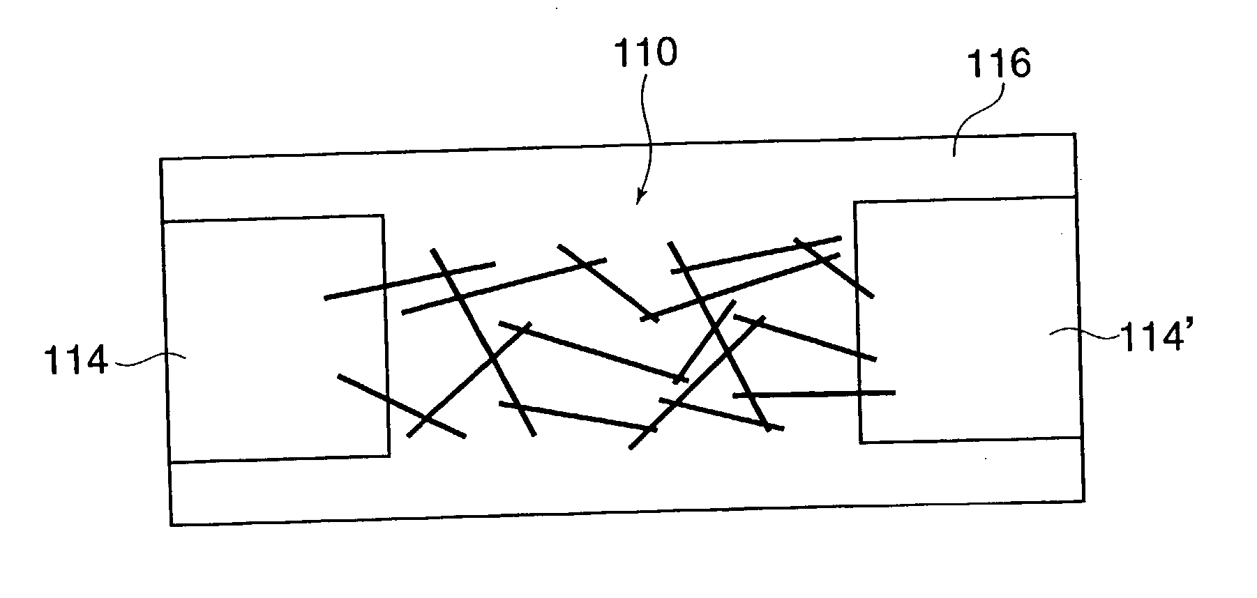
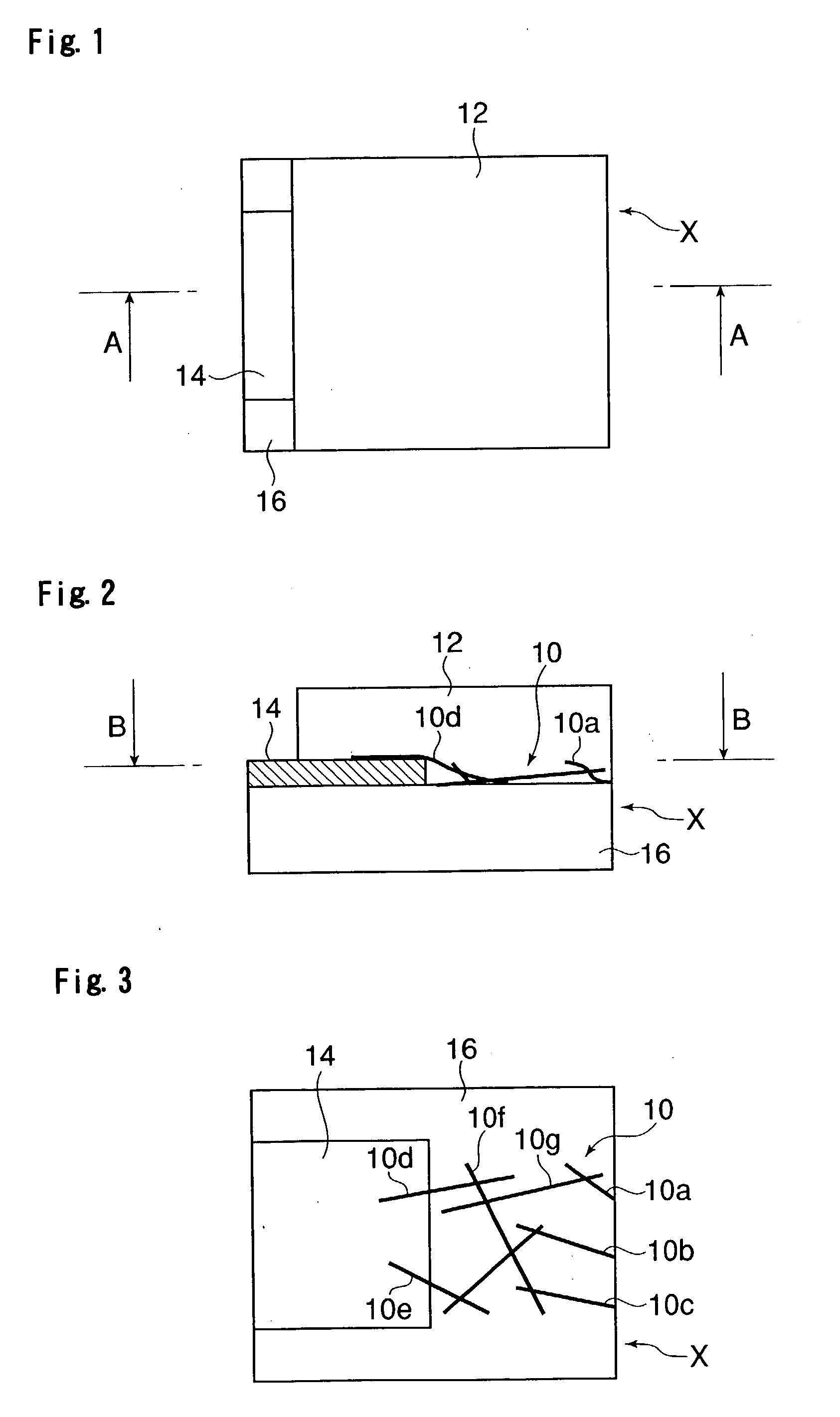
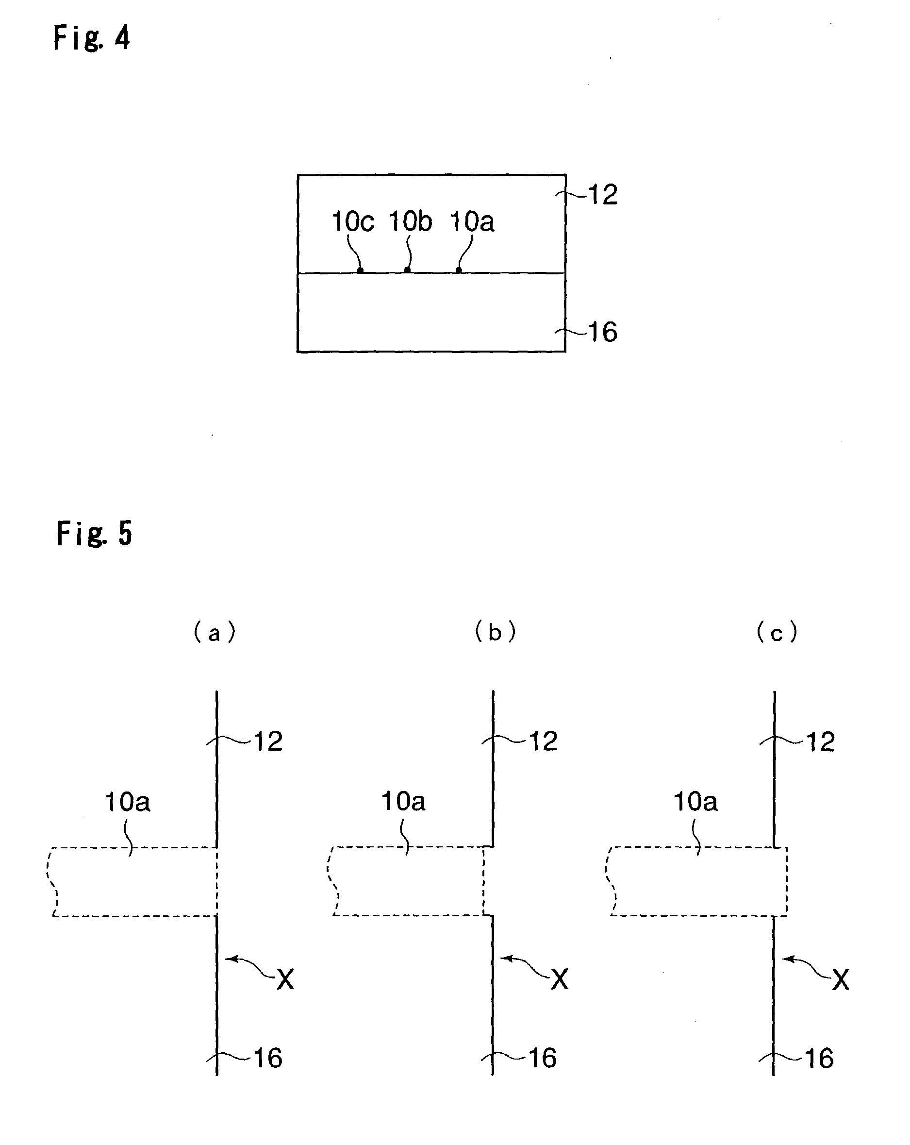
[0199] An electric part useable as a sensor electrode in accordance with Example 1 is manufactured through the processes shown in FIGS. 11 to 17. The details will be described below.

[0200] Au is formed on a surface of a polyimide film that acts as the substrate 116 (20 mm.times.5 mm.times.20 .mu.m, and 1.times.10.sup.12 .OMEGA.cm in volume resistance) in a given region from both the ends through the vapor deposition method, to thereby obtain a state shown in FIG. 11 where the electrodes 114 and 114' (7 mm.times.1 mm.times.about 200 nm, respectively) are formed (electrode layer forming process).

[0201] On the other hand, multi-layer carbon nanotubes that are 20 nm in number average diameter and 3 .mu.m in number average length are added in a dispersion medium with a concentration of 0.1 mass % to prepare a dispersion solution A. The dispersion medium in which a surface active agent (benzalkonium chloride made by Wako Pure Chemical Industries, Ltd.) is added to water with 1 ma...

Example

Comparative Example 1

[0207] An Au electrode is prepared as an electrode of a comparative example, and is set as an electric part of Comparative Example 1. The Au electrode of this comparative example is specifically directed to an electrode in which an Au wire which is 1.6 mm in diameter (purity of 99.9%) is coated with an urethane resin, and only the end portion of the Au wire is exposed.

[0208] The measurement of voltammetry is conducted on the electric part obtained by this comparative example as in Example 1. A graph exhibiting the measured result is shown in FIG. 23. As shown in FIG. 23, it is found that the electric part of this comparative example is not preferable as the high-speed response sensor electrode as in the conventional sensor electrode because it draws the hysteresis curve.

Example

Example 2

[0209] An electric part according to Example 2 is manufactured as in Example 1 except that the carbon nanotubes used in Example 1 is replaced by single-layer carbon nanotubes which are about 1 nm in number average diameter and 3 mm in number average length.

[0210] The measurement of voltammetry is conducted on the electric part obtained by this example as in Example 1. A graph exhibiting the measured result is shown in FIG. 24. As shown in FIG. 24, it is found that the electric part according to this example functions as a sensor electrode that enables a high-speed response without drawing a hysteresis curve.


PUM

PropertyMeasurementUnit
Dispersion potentialaaaaaaaaaa
Electrical resistanceaaaaaaaaaa
Electrical conductoraaaaaaaaaa

Abstract

There are provided an electric part which can be produced through a production process which is excellent in an industrial productivity and a method of manufacturing the electric part, by including a matrix-shaped nonconductive base member, a carbon nanotube group that is sealed within the nonconductive base member and includes one carbon nanotube or plural carbon nanotubes which are electrically connected to each other, in which substantially only end portion of the one carbon nanotube or at least one carbon nanotube contained in the plural carbon nanotubes is exposed from one surface of the nonconductive base member, and an electrode that is connected to a side surface of the at least one carbon nanotube contained in the carbon nanotube group.

Description

FIELD OF THE INVENTION AND RELATED ART STATEMENT[0001] The present invention relates to an electric part which can be used as a rectifier, a sensor electrode, or the like and a method of manufacturing the electric part, and more particularly to an electric part using a carbon nanotube which is low in energy loss and has a novel availability and a method of manufacturing the electric part.[0002] Up to now, because a single layer carbon nanotube exhibits a semiconductor characteristic, an attempt has been made to use the carbon nanotube as an electronic device, and a rectifier and a transistor have been manufactured by using the carbon nanotube by way of trial, and also announced (for example, refer to S. J. Tans et al., "Room-temperature transistor based on a single carbon nanotube", Nature, 1998, vol. 393, pp. 49-52, M. S. Fuhrer et al., "Crossed Nanotube Junctions", Science, vol. 288 (2000), p. 494). Also, there has been reported a technique by which only a single layer carbon nano...

Claims


Application Information

Patent Timeline
IPC IPC(8): B81B1/00B81B7/00B81C1/00B81C99/00H01B1/24H01L21/00H01L31/0312H01M4/02H01M4/66
CPCB81C1/00B82Y10/00B82Y30/00Y10T29/49004H01M4/663H01M2004/022Y10T29/49002H01B1/24Y02E60/10
Inventor WATANABE, MIHOWATANABE, HIROYUKIMANABE, CHIKARASHIMIZU, MASAAKI
Owner FUJIFILM BUSINESS INNOVATION CORP
Why Eureka
Try Eureka