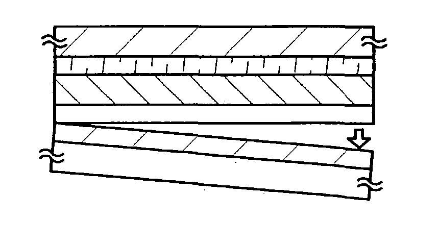
Peeling method

a layering and layering technology, applied in the direction of semiconductor devices, electrical apparatus, transistors, etc., can solve the problems of difficult and heavy cracking, inability to form any tft with electric characteristics, glass substrates, quartz substrates and the like,

Inactive Publication Date: 2004-05-06
SEMICON ENERGY LAB CO LTD
View PDF46 Cites 137 Cited by
  • Summary
  • Abstract
  • Description
  • Claims
  • Application Information

AI Technical Summary

Benefits of technology

[0013] Through a large number of experiments and examinations, the inventors of the present invention have found a peeling method in which, when: a metal layer is provided on a substrate; an oxide layer is formed contacting with the metal layer; an insulating film is formed on the oxide layer; a layer containing hydrogen, typically an amorphous silicon film containing hydrogen, is formed on the insulating film; and heat treatment is performed to the resultant lamination layer at 410.degree. C. or more, while abnormality in the process such as peeling does not occur, peeling can be completely performed with ease at an interface of the oxide layer (interface of the oxide layer and the metal layer) by using physical means, typically performing application of a mechanical force (for example, performing peeling with hand).
[0015] Further, when the oxide layer is formed on the metal layer, a surface of the metal layer is oxidized. Thus, adhesion property between the metal layer and the oxide layer is improved. Then, it is considered that hydrogen contained in the layer containing hydrogen is diffused at 410.degree. C. or more, and the reaction (for example, reduction reaction) of hydrogen and the oxidized surface of the metal layer occurs, whereby the adhesion property between the metal layer and the oxide layer is lowered. In addition, since the stress of the layer containing hydrogen is changed toward a tensile stress through heating, distortion is caused at the interface of the metal layer and the oxide layer, which easily leads to peeling.
[0051] Further, in each of the above-described structures related to the method of manufacturing a semiconductor device, in the case of the manufacture of a light emitting device typified as a light emitting device including an EL element, it is preferable that: the support member is used as a sealing member; and a light emitting element is completely shut off from the outside to avoid the entry of a substance which promotes deterioration of an organic compound layer, such as moisture or oxygen from the outside. Further, when reduction in weight is placed at the highest priority, a film-like plastic substrate is preferably used. However, this exerts a little effect of avoiding the entry of the substance, which promotes deterioration of the organic compound layer, such as moisture or oxygen from the outside. Therefore, there may be adopted, for example, a structure in which a first insulating film, a second insulating film, and a third insulating film are provided on the support member, thereby sufficiently avoiding the entry of the substance which promotes deterioration of the organic compound layer, such as moisture or oxygen from the outside. Note that the second insulating film (stress relaxing film) sandwiched between the first insulating film (barrier film) and the third insulating film (barrier film) is made to have a film stress smaller than that of either the first insulating film or the third insulating film.
[0052] Moreover, in the case of the manufacture of a light emitting device typified as a light emitting device including an EL element, it is preferable that a first insulating film, a second insulating film, and a third insulating film are provided to not only the support member but also the transfer member, which sufficiently avoids the entry of the substance which promotes deterioration of the organic compound layer, such as moisture or oxygen from the outside.

Problems solved by technology

Today, although a glass substrate, a quartz substrate and the like are used in many cases, they have disadvantages that they are easy to crack and heavy.
Further, in terms of mass production, the glass substrate, the quartz substrate and the like are difficult and unsuitable for enlargement.
However, since the heat resistance of the plastic film is low, the highest temperature for process is required to be low and consequently, it is presently impossible to form any TFT with electric characteristics as excellent as those formed on a glass substrate.
In order to transmit energy through the substrate and supply energy sufficient to release hydrogen contained in the amorphous silicon, relatively intense laser beam has to be radiated, resulting in a problem that the layer to be peeled is damaged.
As a result, there is a possibility of insufficient peeling, even if laser beam is radiated to the isolation layer.
Subsequently, attributed to retention of the quantity of hydrogen contained in the isolation layer, there occurs a problem that the process after isolation layer formation may be limited.
In such a case, it becomes difficult to fabricate a transmission type liquid crystal display device.
Additionally, by the above-described method, peeling of the layer to be peeled having a large surface area becomes difficult.
In addition, since the stress of the layer containing hydrogen is changed toward a tensile stress through heating, distortion is caused at the interface of the metal layer and the oxide layer, which easily leads to peeling.
However, this exerts a little effect of avoiding the entry of the substance, which promotes deterioration of the organic compound layer, such as moisture or oxygen from the outside.
Further, a thickness in the vicinity of a peripheral portion of the substrate is likely to be ununiform since the substrate is fixed by sputtering.
As a result, the change was hardly seen through the treatments under all the conditions.
Since the stress is greatly changed with a large thickness of the silicon oxide film, distortion is apt to occur at an interface of the W film and the silicon oxide film, which leads to generation of a peeling phenomenon.
As a result, peeling can not be performed.

Method used


Image

  • Peeling method
  • Peeling method
  • Peeling method

Examples


embodiment 1

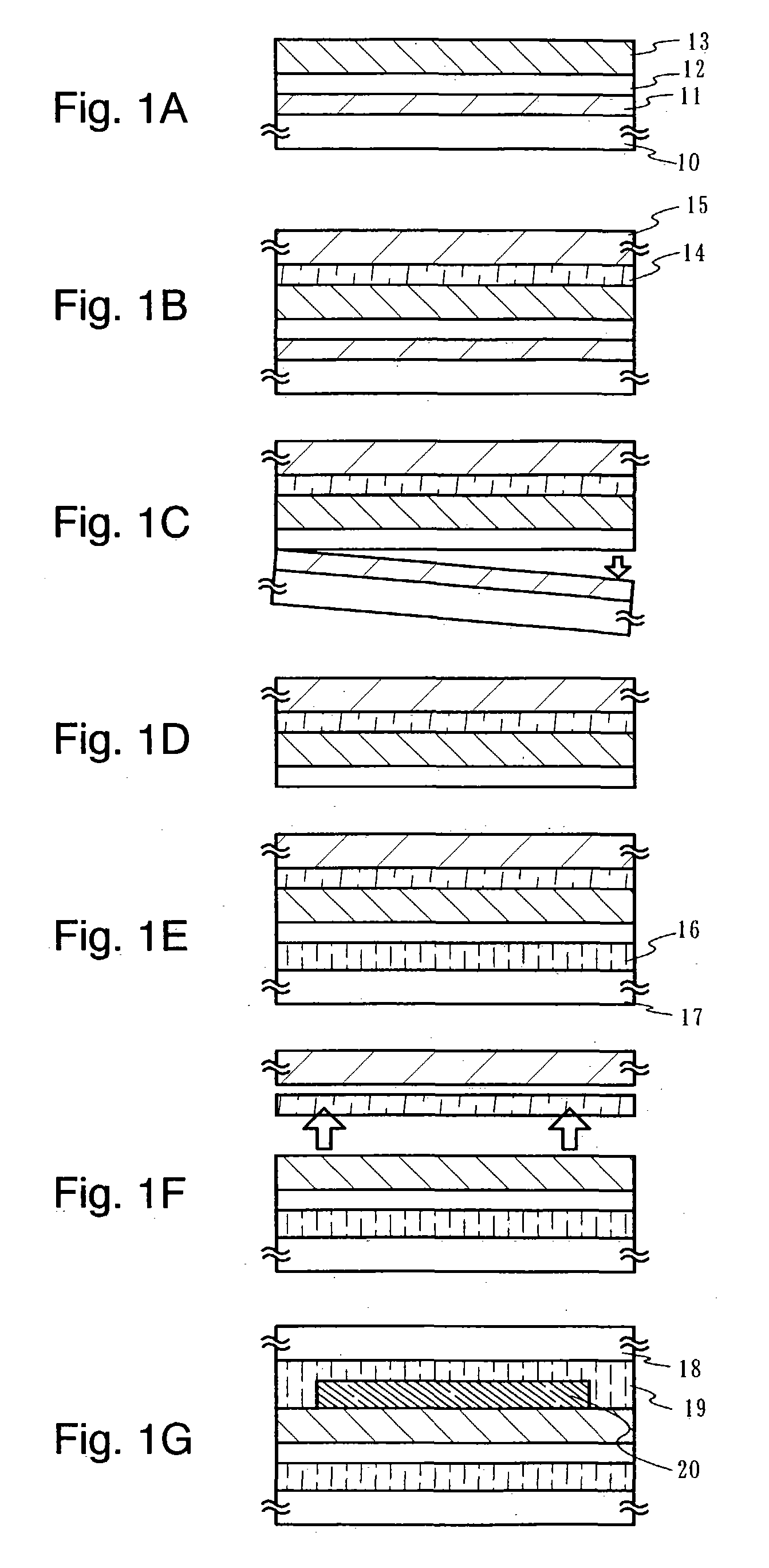
[0100] Embodiments of the present invention will be described with FIGS. 4A to 6. Here, a method of simultaneously manufacturing TFTs (n-channel TFTs and a p-channel TFT) for a pixel portion, and for a driving circuit provided in the periphery of the pixel portion on the same substrate will be described in detail using. Although shown here is an example of manufacturing an active matrix substrate to manufacture a reflective liquid crystal display device, there is no limitation putted thereon. If, appropriately change the arrangement of TFTs and the materials of pixel electrodes, needless to say that it is possible to manufacture either a transmissive liquid crystal display device or a light emitting device having a light emitting layer containing an organic compound.

[0101] A glass substrate is used as a substrate. First, a silicon oxynitride layer is formed of 50 nm thick on the substrate using a PCVD method.

[0102] Subsequently, using sputtering to form a tungsten layer of 50 nm thi...

embodiment 2

[0153] Embodiment 1 shows an example of a reflective display device in which a pixel electrode is formed from a reflective metal material. Shown in this embodiment is an example of transmissive display device in which a pixel electrode is formed from a light-transmitting conductive film.

[0154] The fabricate processes up through the step of forming an interlayer insulating film are identical with the processes of Embodiment 1, and the description thereof is omitted here. After the interlayer insulating film is formed in accordance with Embodiment 1, a pixel electrode 601 is formed from a light-transmitting conductive film. Examples of the light-transmitting conductive film include an ITO (indium tin oxide alloy) film, an indium oxide-zinc oxide alloy (In.sub.2O.sub.3--ZnO) film, a zinc oxide (ZnO) film, and the like.

[0155] Thereafter, contact holes are formed in an interlayer insulating film 600. A connection electrode 602 overlapping the pixel electrode is formed next. The connectio...

embodiment 3

[0158] An example for fabricating a light emitting device that has a light emitting element including an organic compound layer as a light emitting layer, which formed on a plastic substrate will be described in this embodiment with reference to FIG. 8.

[0159] FIG. 8A is a top surface view of a light emitting device and FIG. 8B is a cross-sectional view of Fig, 8A taken along the line A-A'. A dotted line 1101 is a source signal line driving circuit, 1102 is a pixel portion, and 1103 is a gate signal line driving circuit. Reference numeral 1104 is an enclosing substrate and 1105 is a sealing agent. Inside enclosed by the first sealing agent 1105 is filled with a second transparent sealant 1107. The second sealant 1107 is exposed at four corners.

[0160] Reference numeral 1108 is a source signal line driving circuit and a wiring for transmitting signals inputted to the gate signal line driving circuit 1103, and receives a video signal and a clock signal from FPC 1109 as an external input...


PUM


Abstract

A peeling method is provided which does not cause damage to a layer to be peeled, and the method enables not only peeling of the layer to be peeled having a small area but also peeling of the entire layer to be peeled having a large area at a high yield. Further, there are provided a semiconductor device, which is reduced in weight through adhesion of the layer to be peeled to various base materials, and a manufacturing method thereof. In particular, there are provided a semiconductor device, which is reduced in weight through adhesion of various elements, typically a TFT, to a flexible film, and a manufacturing method thereof. A metal layer or nitride layer is provided on a substrate; an oxide layer is provided contacting with the metal layer or nitride layer; then, a base insulating film and a layer to be peeled containing hydrogen are formed; and heat treatment for diffusing hydrogen is performed thereto at 410° C. or more. As a result, complete peeling can be attained in the oxide layer or at an interface thereof by using physical means.

Description

[0001] 1. Field of the Invention[0002] The present invention relates to a peeling method of a layer to be peeled, especially, a peeling method of a layer to be peeled containing various elements. In addition to that, the present invention relates to a semiconductor device comprising a circuit composed of a thin film transistor (hereinafter referred to as TFT) transferred by sticking a separated layer to be peeled to a substrate and its manufacturing method. The invention relates, for example, an electrooptical device such as a liquid crystal module, a light emitting device such as an EL module, and an electronic apparatus containing such devices as components therein.[0003] The term semiconductor device, in this specification, covers any device as a whole capable of functioning by utilizing semiconductor characteristics and an electro optical device, a light emitting device, a semiconductor circuit, and electronic apparatuses are all included in the semiconductor device.[0004] 2. De...

Claims


Application Information

Patent Timeline
Patent Type & Authority Applications(United States)
IPC IPC(8): H01L21/762H01L21/77H01L29/786H01L21/84
CPCH01L21/76251H01L27/1266H01L27/1214H01L27/1218
Inventor TAKAYAMA, TORUMARUYAMA, JUNYAGOTO, YUUGOOHNO, YUMIKOTSURUME, TAKUYAKUWABARA, HIDEAKI
Owner SEMICON ENERGY LAB CO LTD
Why Eureka
Try Eureka