Magnetic semiconductor memory device

a semiconductor and memory device technology, applied in semiconductor devices, digital storage, instruments, etc., can solve problems such as large power consumption

Inactive Publication Date: 2004-06-03
RENESAS TECH CORP
View PDF3 Cites 14 Cited by
  • Summary
  • Abstract
  • Description
  • Claims
  • Application Information

AI Technical Summary

Problems solved by technology

Consequently, there has arisen a problem that power consumption is large.

Method used


Image

  • Magnetic semiconductor memory device
  • Magnetic semiconductor memory device
  • Magnetic semiconductor memory device

Examples


second embodiment

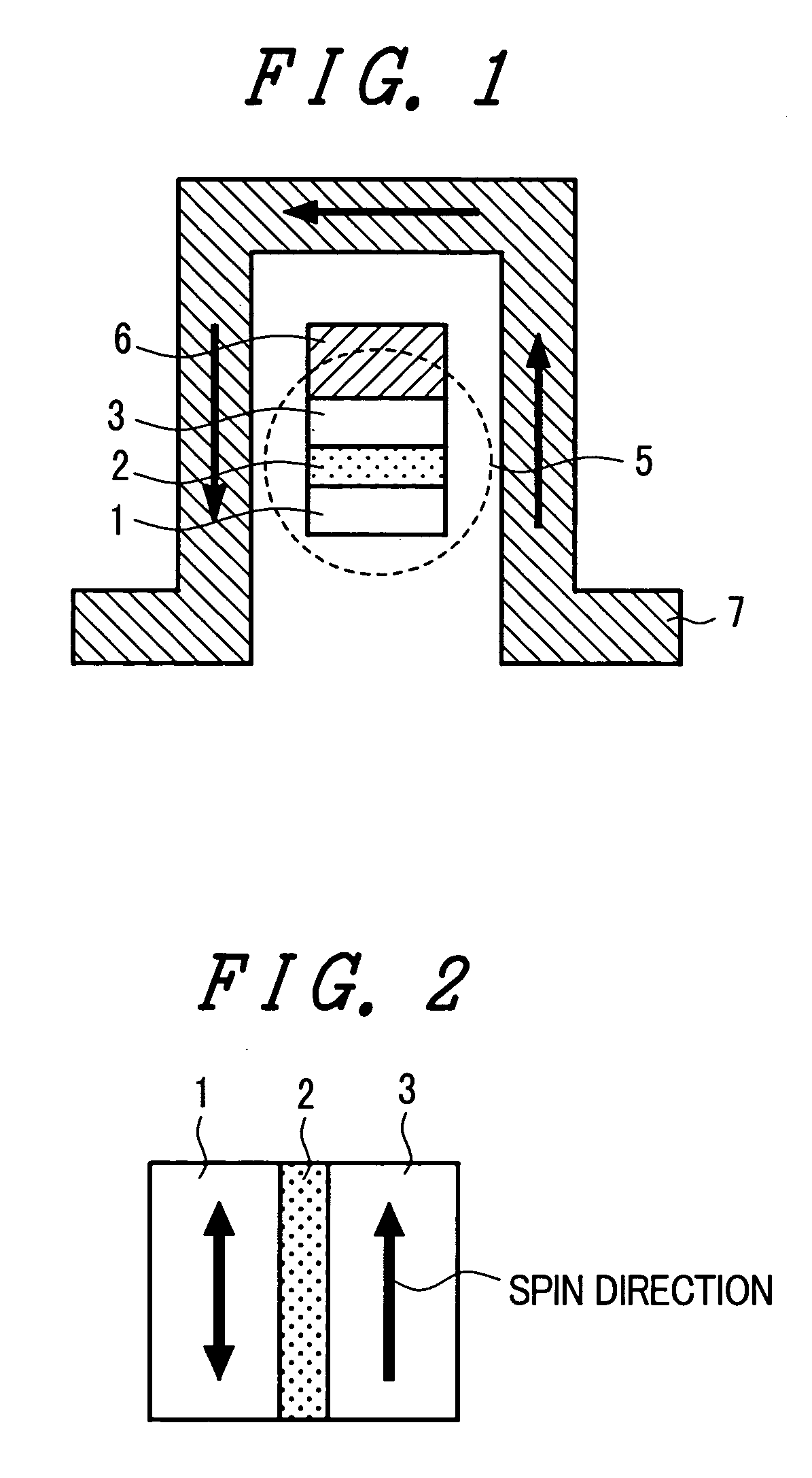
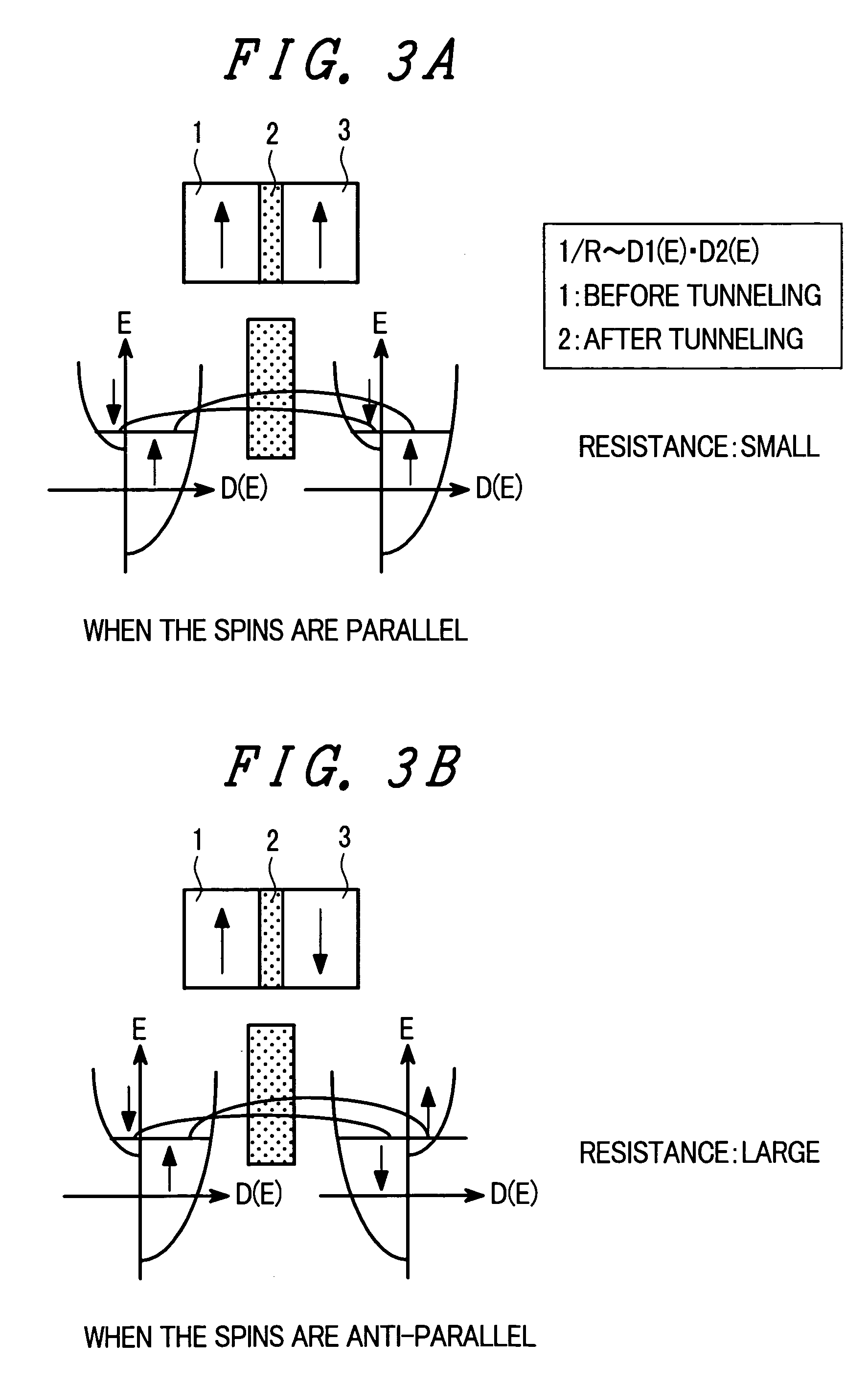
[0056] The present embodiment is directed to a method for achieving power reduction more than in the first embodiment. In order to accomplish the object, a bit line is covered with a soft magnetic material such as NiFe. As a result, it is possible to prevent any leakage of a magnetic field from a portion covered with the magnetic material, so as to generate a stronger magnetic field, thereby achieving power reduction. A fabricating method will be described below in reference to the attached drawings.

[0057] The fore half of the fabricating processes are the same as those in the first embodiment. Specifically, the processes illustrated in FIGS. 9 to 14 are the same as those in the first embodiment. Subsequently, tungsten serving as a bit line is deposited in a thickness of 100 nm. Next, for the purpose of magnetic shield, a soft magnetic material 21 such as NiFe is deposited in a thickness of 10 nm. Furthermore, a silicon oxide film is deposited in a thickness of 100 nm. The resultant...

third embodiment

[0062] In the first and second embodiments, the normal planar transistor is used as the select transistor in the MRAM. In the present embodiment, a vertical transistor is used as the select transistor, thereby reducing a cell area. Unlike the DRAM, a leak current in a cell transistor cannot critically influence on a memory function in the MRAM. This is because information is held in the spin direction. Thus, in the present embodiment, processes are simplified by forming the vertical transistor with polycrystalline silicon. Hereinafter, explanation will be made in reference to the attached drawings.

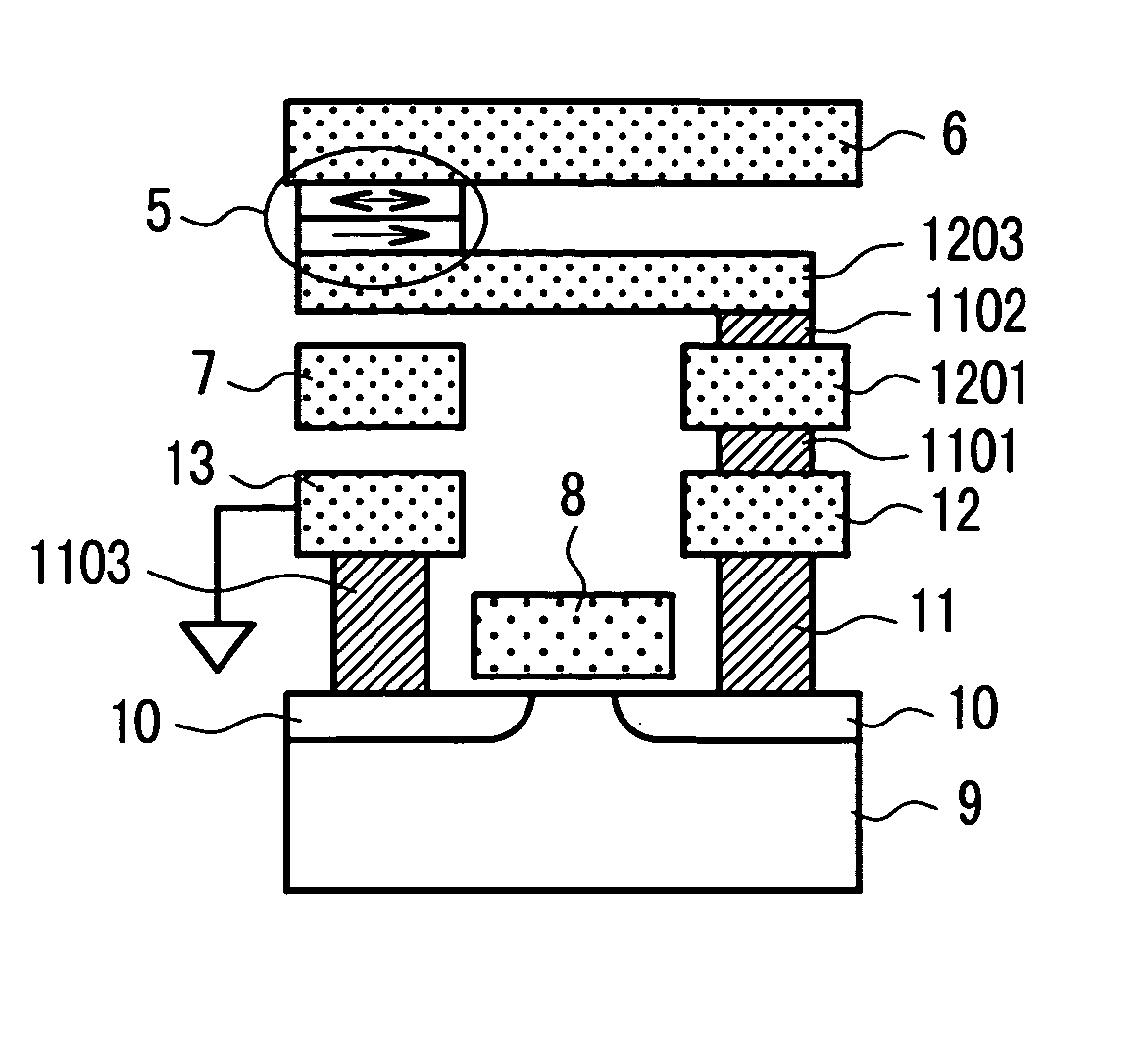
[0063] A transistor in a peripheral circuit is formed in normal fabricating processes. After the deposition of an interlayer dielectric 17, a contact plug is fabricated, and further, a first local wiring made of tungsten is formed. In a memory array, the resultant wiring layer is used as a common ground line 13. The state at this time is shown in FIG. 26. Subsequently, an interlayer dielec...


PUM


Abstract

A memory cell in a so-called MRAM by utilizing a tunnel magnetic resistance in the prior art has raised problems that a magnetic field to be applied to a TMR element is essentially weak since a word line for write is disposed apart from the TMR element, that a large current is required at the time of a writing operation, and that electric power consumption is large. In order to solve the above-described problems experienced in the prior art, the present invention provides an MRAM memory cell structure and its fabricating method in which a word line for write is disposed near a TMR element and surrounds it in three directions.

Description

[0001] 1. Field of the Invention[0002] The present invention relates to a semiconductor memory device. In particular, the present invention relates to a fast non-volatile random access memory (RAM) by utilizing a magneto resistance effect.[0003] 2. Description of the Related Art[0004] Expectations have been raised on an MRAM (a magnetic random access memory) as a next generation fast non-volatile memory provided with merits of both of a DRAM and a FLASH, which are typical semiconductor memories for the present.[0005] The MRAM is a fast non-volatile memory by utilizing a tunnel magneto resistance (TMR) of a ferromagnetic spin tunnel junction (MTJ). Since IBM has announced that a memory of 256 M bit will be produced in 2004 in cooperation with Infineon, such a memory has become a focus of attention. On the academic level, Motorola tried to fabricate an array of 1 MB and reported the confirmation of memory operation in 2002 Symposium on VLSI Circuits Digest of Technical Papers, pp. 160...

Claims


Application Information

Patent Timeline
Patent Type & Authority Applications(United States)
IPC IPC(8): G11C11/15G11C11/16G11C29/00H01L21/8246H01L27/105H01L43/08
CPCG11C11/16
Inventor MATSUOKA, HIDEYUKIITO, KENCHISAKATA, TAKESHIITOH, KIYOO
Owner RENESAS TECH CORP
Why Eureka
Try Eureka