Manufacturing method for semiconductor device

a manufacturing method and technology for semiconductor devices, applied in semiconductor devices, instruments, electrical equipment, etc., can solve the problems of inability to precisely control the conditions of the etching process, the low withstanding pressure of the film transistor using a polycrystalline silicon film, and the uneven shape of each shap

Inactive Publication Date: 2004-09-02
SEMICON ENERGY LAB CO LTD
View PDF28 Cites 9 Cited by
  • Summary
  • Abstract
  • Description
  • Claims
  • Application Information

AI Technical Summary

Problems solved by technology

However, a defect is pointed out that a thin film transistor (TFT) using a polycrystalline silicon film has a low withstanding pressure in drain junction to increase junction leak current (hereinafter, OFF-leak current).
If the selection ratio is low, a portion that needs no etching is etched to have problems that a desired shape cannot be obtained and each shape is not uniform.
In addition, conditions in the process of the etching process cannot be controlled precisely.
Consequently, reliability of a semiconductor device is lowered and yield is also decreased.
In addition, titanium is more costless than expensive tungsten, which is widely used.

Method used


Image

  • Manufacturing method for semiconductor device
  • Manufacturing method for semiconductor device
  • Manufacturing method for semiconductor device

Examples


embodiment 1

[0058] (Embodiment 1)

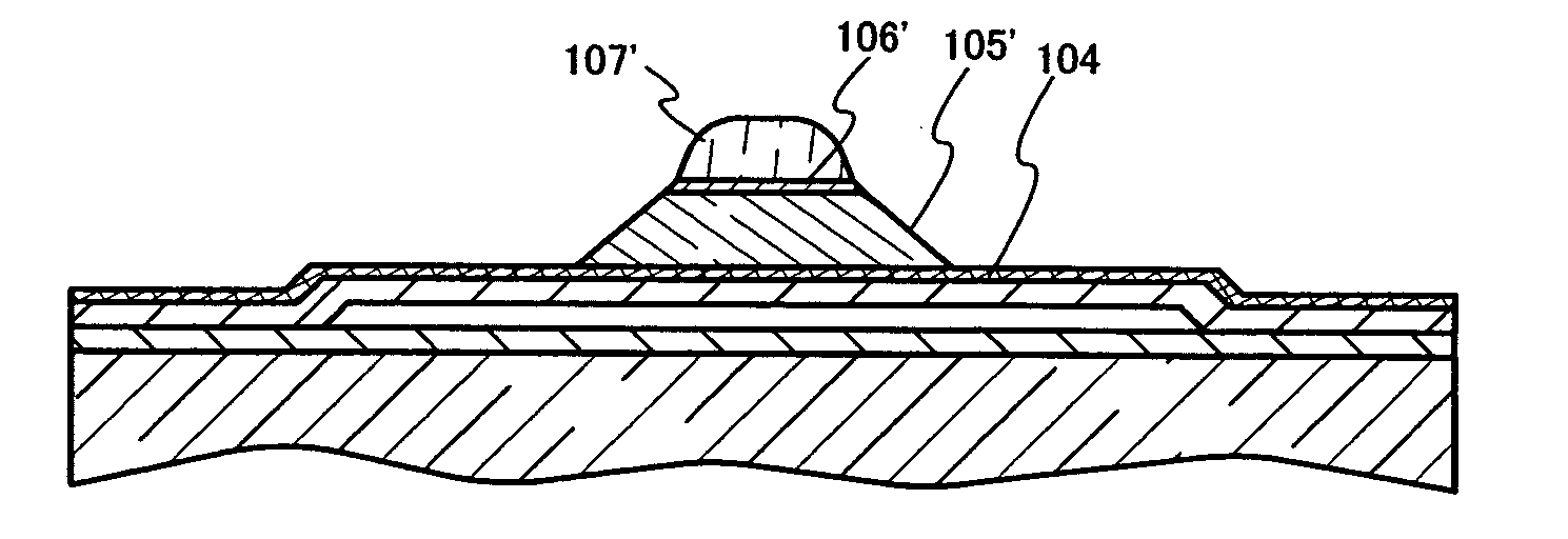
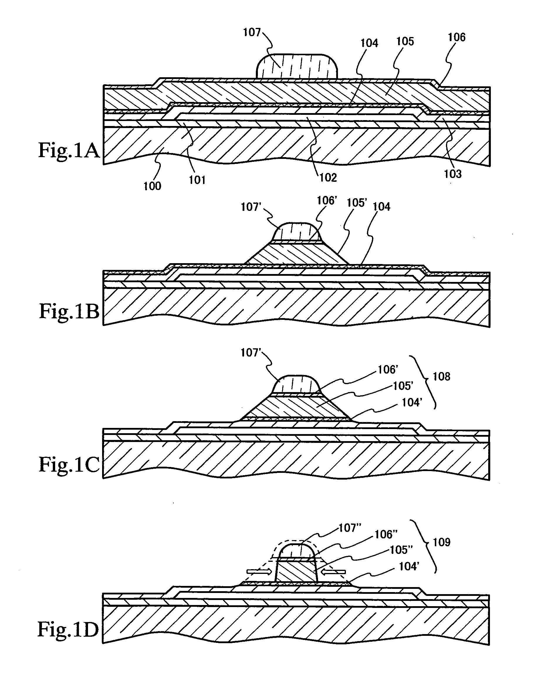
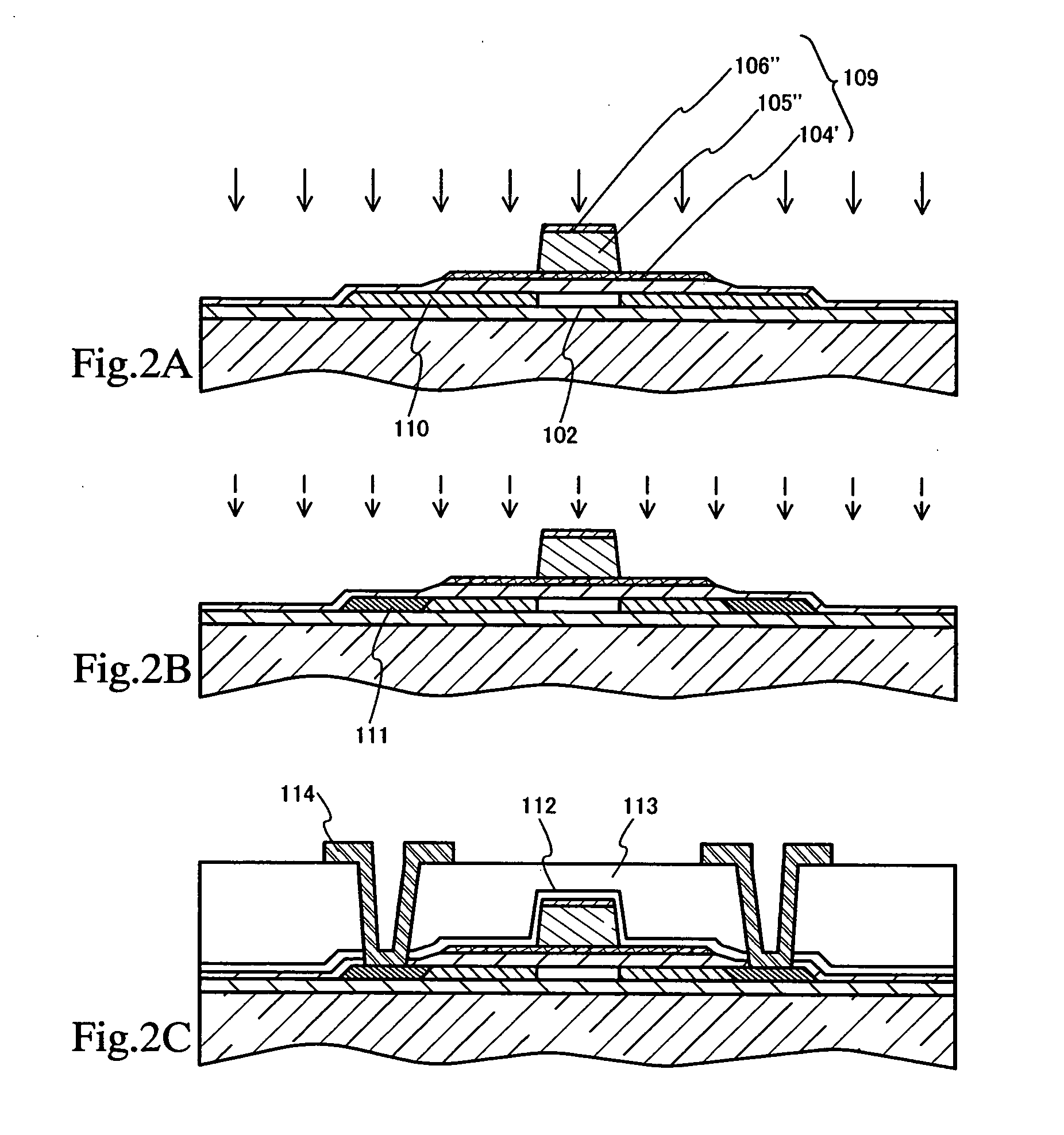
[0059] In the present embodiment, an example of forming a gate electrode according to a process based on the embodiment mode will be described. The present embodiment will be described with reference to FIG. 1A to FIG. 2C. In the present embodiment mode, a semiconductor device with Lov from 1 to 1.5 .mu.m, which is a length necessary for driving a TFT with a channel length on the order of 10 .mu.m at 10 to 20 V, is manufactured. However, the length may be appropriately set depending on a channel length and a driving voltage, and is not limited to the present embodiment. When a method for manufacturing a semiconductor device, according to the present invention, is employed, it is possible to control a length of Lov precisely and manufacture a semiconductor device that has favorable characteristics and high reliability with high yield.

[0060] First, the first insulating layer 101 is formed of a silicon oxynitride film of 150 nm in thickness on the aluminosilicate-g...

embodiment 2

[0075] (Embodiment 2)

[0076] The present invention can apply to semiconductor devices in which various display screens are provided.

[0077] FIG. 12 is a structural example of a semiconductor device that has a display panel 901 mounted in a casing 900, which is applicable to television receivers and monitor systems of computers. In the casing 900, an electronic circuit board 902 and a speaker 903 for sound reproduction are loaded, wherein the electronic circuit board 902 incorporates an amplifier and a high-frequency circuit formed of a semiconductor integrated circuit, and a semiconductor memory or a magnetic memory such as a hard disk as a memory function to fulfill a function of displaying an image.

[0078] A display panel 901 can be comprising a driver-integrated type in which an active matrix pixel circuit 904 in which gate overlapping TFTs according to the present invention are used to arrange the TFT in a matrix shape, a scanning line driving circuit 905, and a data line driving c...


PUM

PropertyMeasurementUnit
voltageaaaaaaaaaa
voltageaaaaaaaaaa
voltageaaaaaaaaaa

Abstract

It is an object of the present invention to enhance a selection ratio in an etching process, and provide a method for manufacturing a semiconductor device that has favorable uniform characteristics with high yield. In a method for manufacturing a semiconductor device according to the present invention, a semiconductor layer is formed, a gate insulating film is formed on the semiconductor film, a first conductive layer is formed on the gate insulating film, a second conductive layer is formed on the first conductive layer, the first conductive layer and the second conductive layer are etched to form a first conductive-layer pattern, the second conductive layer in the first conductive-layer pattern is selectively etched with plasma of boron trichloride, chlorine, and oxygen to form a second conductive-layer pattern, and a first impurity region and a second impurity region are formed in the semiconductor layer.

Description

[0001] 1. Field of the Invention[0002] The present invention relates to a method of manufacturing a semiconductor device. In particular, the present invention relates to a technique of processing a gate electrode of the semiconductor device with etching to form an impurity region in a semiconductor layer.[0003] 2. Description of the Related Art[0004] In a display device using liquid crystal, a part with a large-screen over 20 inches, which is typified by a liquid crystal display TV, has been put to practical use. In recent years, a liquid crystal display device integrated with a driving circuit has been realized with a TFT in which a polycrystalline silicon film is used as an active layer.[0005] However, a defect is pointed out that a thin film transistor (TFT) using a polycrystalline silicon film has a low withstanding pressure in drain junction to increase junction leak current (hereinafter, OFF-leak current). It is known that it is effective to form a lightly doped region (LDD) s...

Claims


Application Information

Patent Timeline
Patent Type & Authority Applications(United States)
IPC IPC(8): H01L21/3065H01L21/336H01L27/12H01L29/423G02F1/1368H01L29/49H01L29/786
CPCH01L29/42384H01L29/4908H01L29/78627H01L29/78621H01L29/66757
Inventor MONOE, SHIGEHARUYOKOSHIMA, TAKASHISASAGAWA, SHINYA
Owner SEMICON ENERGY LAB CO LTD
Why Eureka
Try Eureka