Eureka AIR delivers breakthrough ideas for toughest innovation challenges, trusted by R&D personnel around the world.

Multi-rate analog-to-digital converter

a multi-rate analog-to-digital converter technology, applied in the field of analog-to-digital converters, can solve the problems of increasing the size of the circuit or radio, adding complexity, and affecting the noise floor so as to improve the noise floor level of the multi-rate analog-to-digital converter, improve the noise floor level, and achieve the effect of high degree of generating accuracy

Inactive Publication Date: 2005-01-06
MOTOROLA INC +1
View PDF4 Cites 10 Cited by
  • Summary
  • Abstract
  • Description
  • Claims
  • Application Information

AI Technical Summary

Benefits of technology

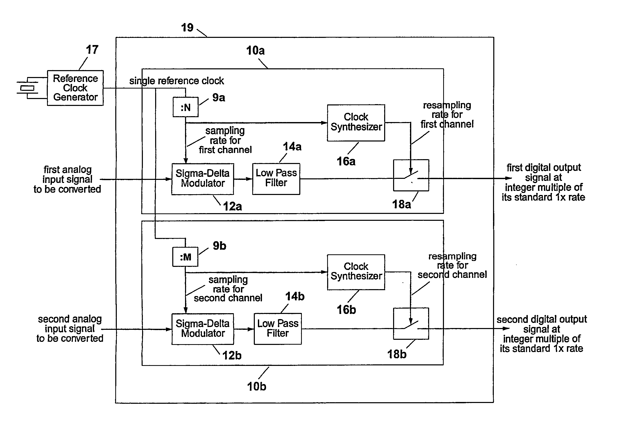
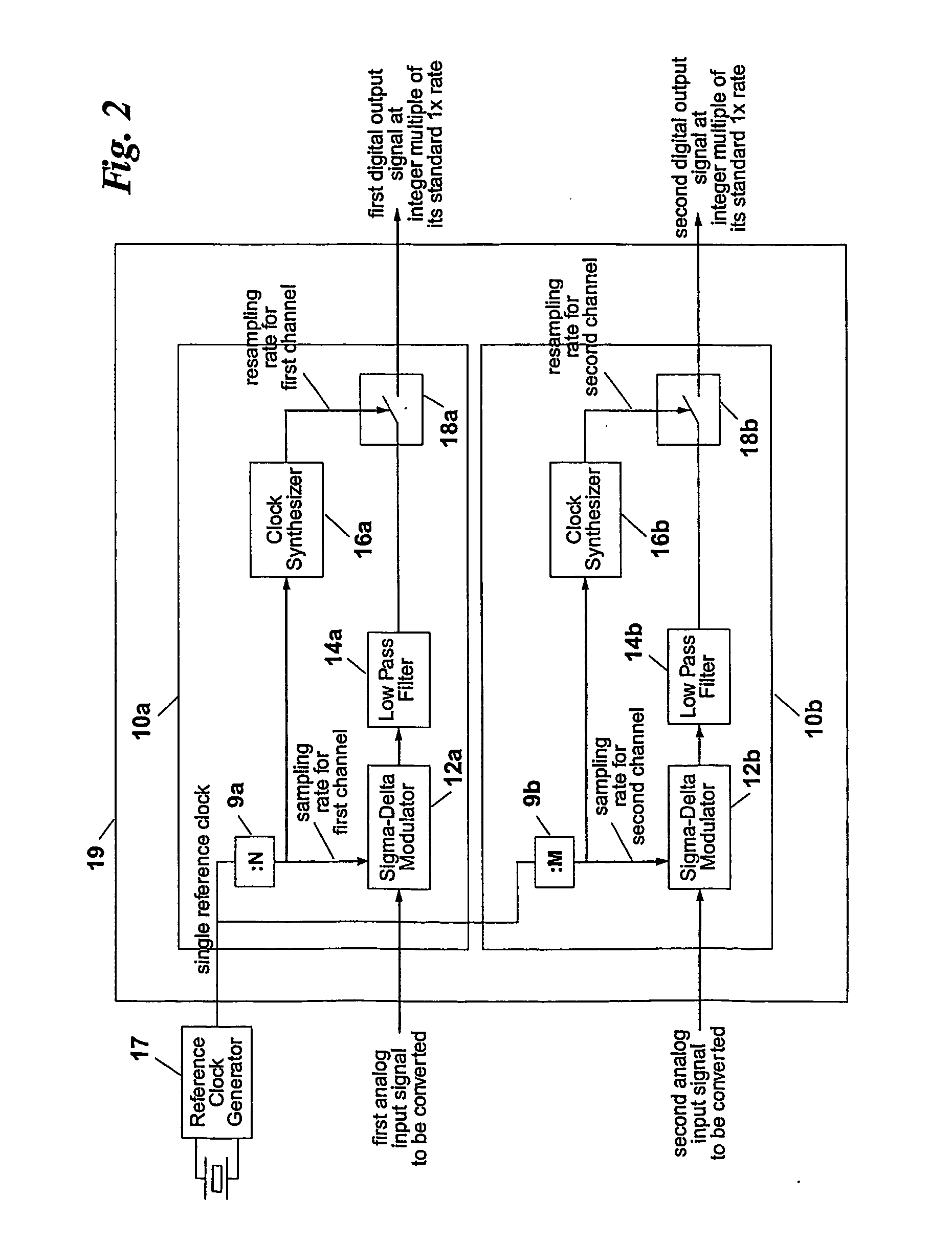
As there is sampling in the digital domain the advantages associated with signal processing, speed and low noise injection are obtained. Similarly as the output of the Sigma-Delta modulator is in digital form, it may be manipulated and processed readily and with existing software. Furthermore as Sigma-Delta modulators tend to oversample: that is they tend to sample at frequencies in excess of the Nyquist rate; configuration of the decimators is relatively straightforward and this greatly eases post processing of the Sigma-Delta modulator output signal. An advantage of this is that there is no longer a requirement to include an additional PLL for each mode of a multi-mode receiver.
Provided the ratio between the sampling rate of the Sigma-Delta modulator and the 1× rate of the standard signal converted by each channel is sufficiently large (typically larger than 8), then any quantisation noise occurring in the Sigma-Delta modulator is kept to a minimum in the desired signal band. Decimation is then advantageously carried out between the data source, that is the Sigma-Delta modulator output, and the data sink, namely the output of the resampler. The decimation process provides low pass filtering which may remove as much as needed of any out-of-band noise, such that harmonics of square wave signals re-sampling the output signal at the desired output rate, will only remove or fold a negligible contribution of the out-of-band noise in the desired signal band at the time re-sampling is done.
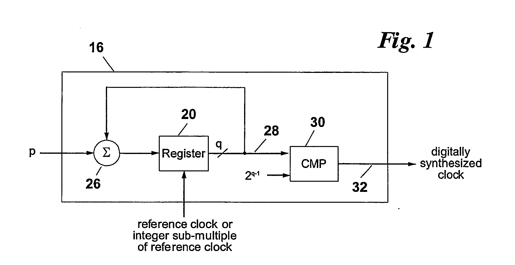
If q is large enough then it is possible to obtain a high degree of accuracy in generating the resampling signal in the relevant mode.
Sample rate conversion (SRC) can impose significant demands upon a Digital Signal Processor (DSP) because interpolators and decimators are employed. However, inclusion of a low pass filter (LPF) in any Sigma-Delta converter enables decimation. As a result of the oversampling and quantisation noise shaping that occur in the modulator, decimation drastically attenuates the noise components that may fall into the desired signal band after resampling. The inventors have realised that this feature may be employed to improve the noise floor levels of a Multi-Rate Analog-to-Digital Converter as well as reduce any aliasing that may occur.
By including a low pass filter (LPF) at the output of the, or each, Sigma-Delta modulator, a lower sampling rate can be achieved at the re-sampler, for example from a system clock frequency of 30.72 MHz to a choice of lower frequencies. The clock synthesiser is coupled to a clocked control switch and advantageously is able to vary the rates at which clocking occurs. Effectively therefore a variable frequency clock is achievable. Typically the clock rate is 270.833 kHz or 541.666 kHz for the GSM channel.
Resampling the signal at a rate close to or equal to the 1× rate of the standard signal in each channel avoids the need for introducing a new high frequency reference clock and associated problems of harmonic interference between several high frequency reference clocks.

Problems solved by technology

However, these not only add complexity, but also increase the size of the circuits or radios.
Furthermore when the frequencies are high, there is a risk that they mix together due to parasitic coupling.
This is highly undesirable because a large spectrum of frequencies is inherent in a clocked square wave, it is likely that some harmonic frequencies which are generated will interfere one with another.
However, no advantage is taken to reduce the processing requirements of components such as oscillators or phase locked loops (PLL's).
Furthermore there is no teaching provided which overcomes the problem associated with operating using two different reference clocks.
A reason for this may be that implementation of some of these alternatives are not always straightforward.
For example a single crystal oscillator, in conjunction with a phase locked loop (PLL) has the disadvantage of introducing analog signals, with associated noise problems.
Moreover, these proposed techniques require using both interpolators and decimators which represents a significant increase in of signal processing and cost.

Method used


Image

  • Multi-rate analog-to-digital converter
  • Multi-rate analog-to-digital converter
  • Multi-rate analog-to-digital converter

Examples


Embodiment Construction

Referring to the Figures, FIG. 1 shows a diagrammatical representation of a Clock Synthesizer 16. The input parameter, p, is selected according to the main clock (not shown) frequency, fref / α, the output frequency to generate, fx, and the number of bits, q, used to accumulate the phase of the output clock signal. A register 20 receives an input from adder 26 and is activated by an input clock which is an integer sub-multiple of the reference clock (not shown). Alternatively the register could be clocked by the reference clock itself. Consequently, the frequency of the clock activating register 20 is given by fref / α, where α is an integer number larger or equal to 1. Register 20 is part of a closed loop also comprising the adder 26. The closed loop accumulates a phase count by means of an increment, p, added to another input of the adder 26. The register 20 presents its output 28 to a Comparator 30. Comparator 30 compares output from register 20 with a value derived from 2q−1. Outpu...


PUM


Abstract

A Multi-Rate Analog-to-Digital Converter (19) is coupled to a single crystal oscillator (17) as a reference clock and has at least two separate channels arranged to sample and convert input data at two differing clock rates. Each channel derives a clock signal from the reference clock. Associated with each of the channels is a Sigma-Delta converter (10a, 10b) comprising a modulator (12), a filter (14) and a resampler (18). The modulator (12) receives input data and provides a data signal to the filter (14), which itself provides a filtered data signal to the associated data resampler. The data resampler resamples the data and provides a digital output signal. As there is sampling in the digital domain the advantages associated with signal processing, speed and low noise injection are obtained. Similarly as the output of the modulator (12) is in digital form, it can be manipulated and processed readily and with existing software.

Description

BACKGROUND OF THE INVENTION This invention relates generally to Analog to Digital Converters (ADC's) and more particularly to Multi-Rate ADC's. Analog to Digital Converters (ADC's) are used in a myriad electronic devices. An example of one type of device that incorporates an ADC is a multi-mode receiver. A multi-mode receiver is used in telecommunication equipment such as a mobile telephone or digital tuner. Multimode receivers use crystal oscillators to generate a single output frequency referred to as a clock frequency. Different carrier signals require different clock frequencies in order to demodulate them. The clock frequencies and other protocols vary according to different standards. For example, the GSM standard requires clocks to operate at 270.833 kHz or at multiples thereof, whereas Wideband Coded Divisional Multiplexed Access standard (WCDMA) operates at 3.84 MHz or multiples thereof. Because there is no direct way of deriving one frequency from another, multi-mode de...

Claims


Application Information

Patent Timeline
Patent Type & Authority Applications(United States)
IPC IPC(8): H03M3/00H03M3/02
CPCH03M3/496
Inventor CLEMENT, PATRICKKHLAT, NADIMSCHWARTZ, DANIEL B.
Owner MOTOROLA INC
Why Eureka
Eureka Blog
Learn More