Time resolved emission spectral analysis system

a technology of emission spectrum and analysis system, which is applied in the direction of optical radiation measurement, instruments, spectrometry/spectrophotometry/monochromators, etc., can solve the problems of light emission and failure of locating semiconductor devices, and achieve the effect of high spatial resolution and noise reduction

Inactive Publication Date: 2005-01-06
ONTONICS
View PDF15 Cites 59 Cited by
  • Summary
  • Abstract
  • Description
  • Claims
  • Application Information

AI Technical Summary

Benefits of technology

[0018] In another aspect of the invention, the inventive system comprises an x-y-z stage that is used to move the optics to the location of interest on the device under test, and focus and image the device(s) of interest. The navigation is performed in relation to a CAD layout of the IC. A mechanized shutter is used to variably define imaging areas within the field of view of the optics. During navigation and target acquisition, the device is illuminated and is imaged with an imaging array, thereby providing high spatial resolution. When a device to be tested has been aligned, i.e., placed within the imaging area, the illumination source is turned off and the device is electrically stimulated with test signals. During the stimulation period, hot electron photon emission, as well as photon emission from other sources such as hot holes, gate leakage, and oxide tunneling, is collected by the optics and is imaged onto the core of a multimode optical fiber. The collected light is filtered to a predefined optical bandwidth before it is sensed by a detector, thereby providing spectral resolution.
[0019] To provide the temporal resolution, emission detection is synchronized with the test signals, i.e., the automated test equipment (ATE). The detector is coupled to a time-resolved photon counting detector, such as one comprising an avalanche quenching circuit, a time-to-amplitude converter (TAC), and a multi-channel analyzer. Optionally, the APD is gated so that it assumes the detection condition only just before a light emission is expected according to the sync signal from the ATE. This provides reduction in noise.

Problems solved by technology

For example, avalanche breakdown in insulators causes light emission, and detection of such light emission can point to the locations of failure in the device.
Various emission microscopes have been used for detecting locations on the device where the electrical current drawn exceeds the expected levels and therefore could lead to locating failures in semiconductor devices.

Method used


Image

  • Time resolved emission spectral analysis system
  • Time resolved emission spectral analysis system
  • Time resolved emission spectral analysis system

Examples


Embodiment Construction

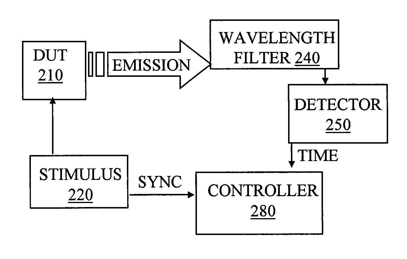
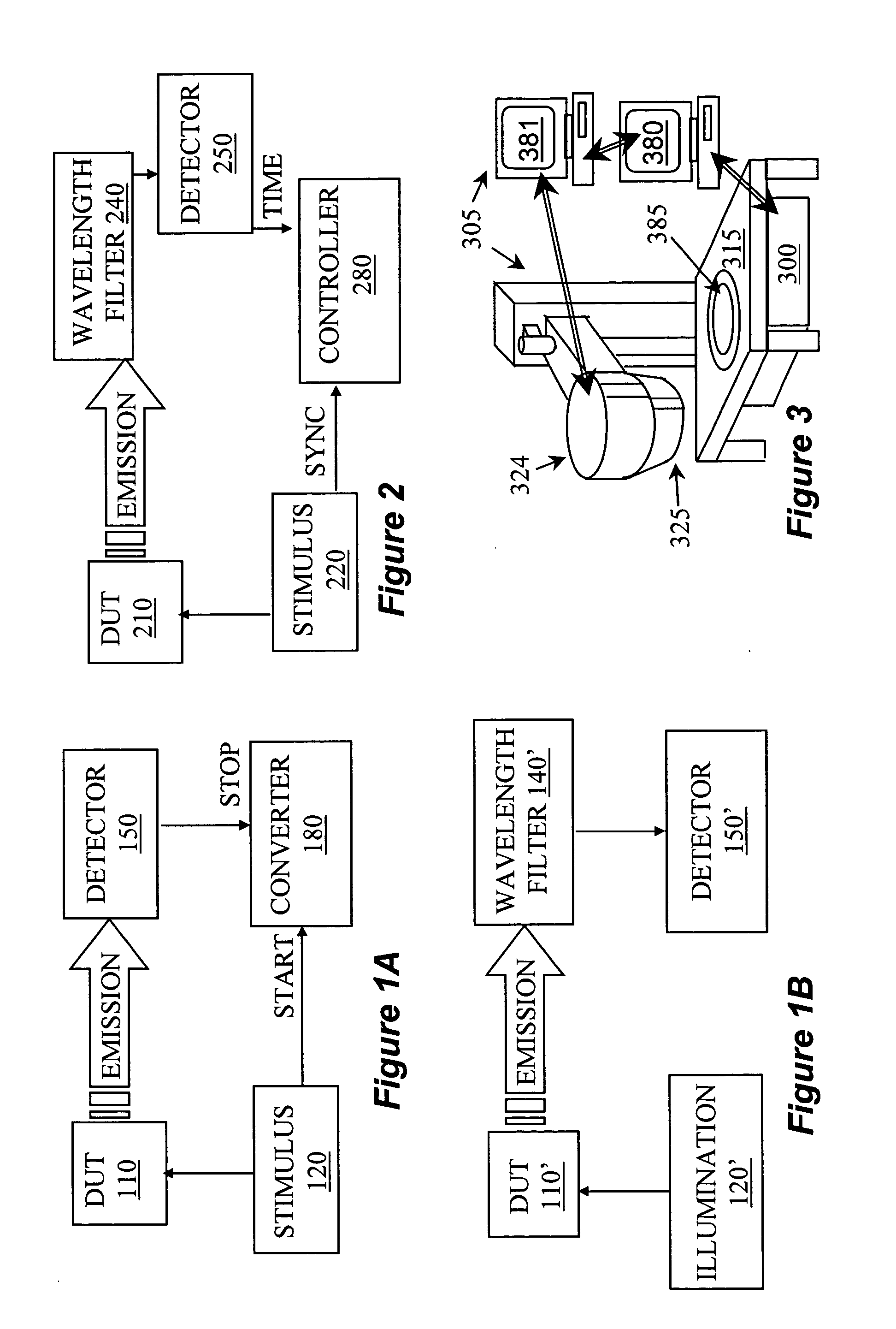
[0030] The present invention provides a testing and debug system particularly suitable for rise time, timing, logic fault localization, and other testing of microchips. The investigation is performed with respect to a time correlation to electrical stimulus provided to the DUT, and with respect to the wavelength of the light emitted from the DUT. FIG. 2 is a block diagram depicting the major components of the system according to an embodiment of the invention. The ATE 220 electrically stimulates the DUT 210, and also sends a sync signal to the controller 280. In response to the stimulus, DUT 210 provides optical emission, which is made to pass through a wavelength filter 240. Selected wavelengths pass through the filter 240 and are directed to detector 250. The signal from the detector 250 is sent to the controller 280. Consequently, the system provides temporal and spectral resolution of optical emission of the DUT.

[0031] By studying time-correlated emission at particular waveleng...


PUM


Abstract

A system for temporal and spectral resolved detection of photon emission from an integrated circuit is disclosed. A DUT is stimulated by a conventional ATE, so that its active devices emit light. The signal from the ATE is also sent to the system's computer as a synchronization signal. The light emitted from the switching devices is passed through a wavelength filter. Selected bands of wavelengths are then passed to respective detector(s) and the detector(s) response with respect to the time correlated ATE stimulus is studied.

Description

BACKGROUND OF THE INVENTION [0001] 1. Field of the Invention [0002] The present invention relates to a system for in-situ transistor level measurement of emission spectral and timing information directly related to the switching events (logic transitions) of electrically active semiconductor integrated circuits. [0003] 2. Description of the Related Art [0004] It is known in the prior art that various mechanisms in semiconductor devices can cause light emission. Detection of such light emission has been used to investigate semiconductor devices. For example, avalanche breakdown in insulators causes light emission, and detection of such light emission can point to the locations of failure in the device. Similar detection can be used to characterize electrostatic discharge in the device. In electrically stimulated (active) transistors, accelerated carriers (electrons & holes), i.e., hot-carriers, emit light when the device draws current. Various emission microscopes have been used for ...

Claims


Application Information

Patent Timeline
Patent Type & Authority Applications(United States)
IPC IPC(8): G01R11/24
CPCG01R31/311
Inventor KASAPI, STEVENWOODS, GARY LEONARDFIELD, JOHN E.
Owner ONTONICS
Why Eureka
Try Eureka