Method of and apparatus for manufacturing semiconductor thin film, and method of manufacturing thin film transistor

Inactive Publication Date: 2005-01-06
VISTA PEAK VENTURES LLC
View PDF8 Cites 61 Cited by
  • Summary
  • Abstract
  • Description
  • Claims
  • Application Information

AI Technical Summary

Benefits of technology

[0044] According to the method and the apparatus for manufacturing the semiconductor thin film in the present invention, the following effects can be attained. That is, the width of the crystal along the second direction can be made larger than that of a conventional semiconductor thin film, because of the temperature gradient generated along the second direction. Moreover, the positions of the grain boundaries can be controlled, and also the number of the grain boundaries can be reduced. Also, the positions and the number of the crystals can be controll

Problems solved by technology

However, if there are a large number of grain boundaries in the poly-silicon film 102, the mobility of the carrier decreases, which results in a problem that the mobility of the TFT can not be made faster.
However, there is a problem with this technique in that the formation of the grain boundaries can not be controlled, even though the growth direction of the crystal can be controlled to some degree.
If the grain boundary crosses the channel portion of the thin fi

Method used


Image

  • Method of and apparatus for manufacturing semiconductor thin film, and method of manufacturing thin film transistor
  • Method of and apparatus for manufacturing semiconductor thin film, and method of manufacturing thin film transistor
  • Method of and apparatus for manufacturing semiconductor thin film, and method of manufacturing thin film transistor

Examples


Example

FIRST EXAMPLE

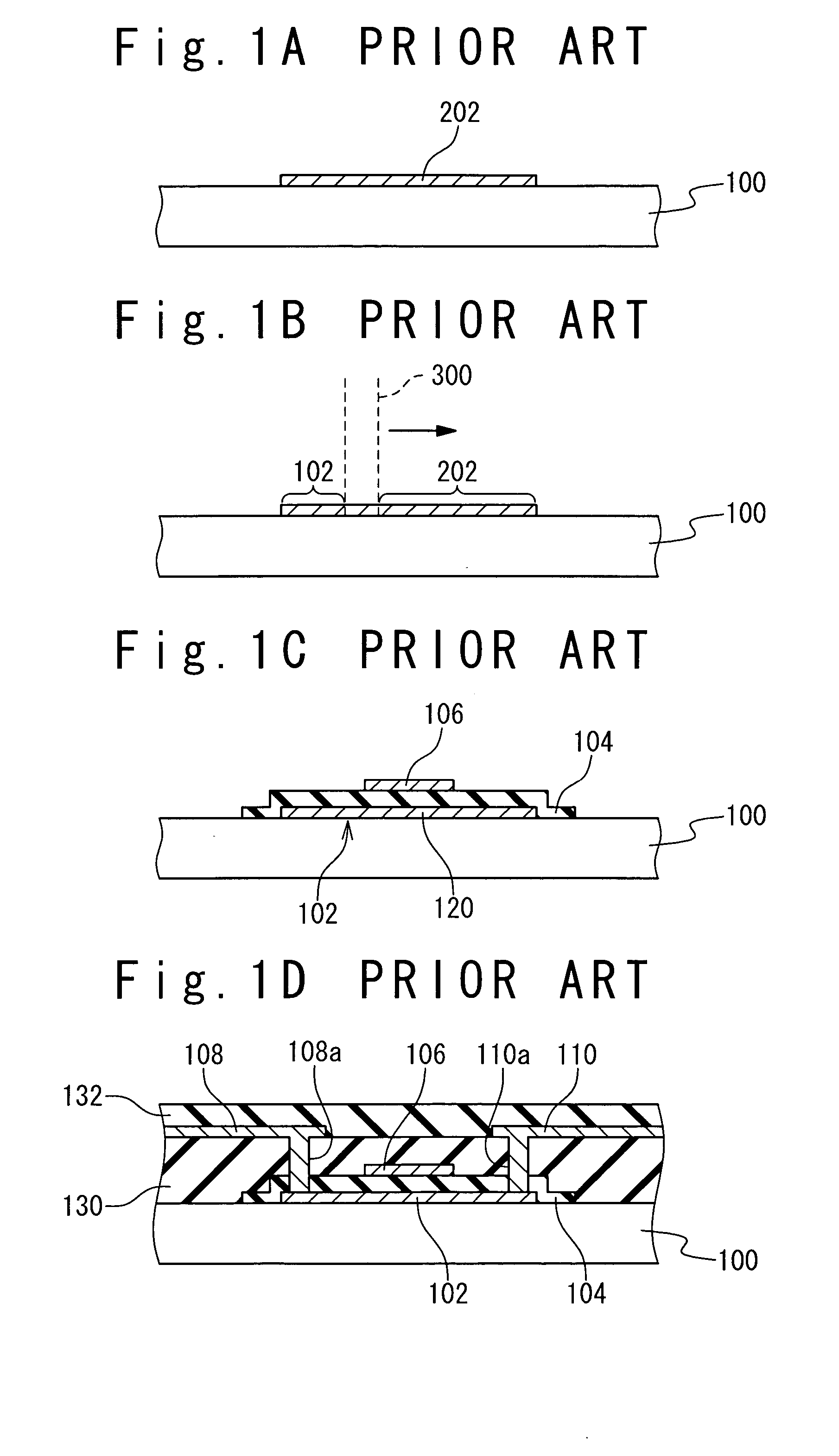
[0095]FIG. 12 is a schematic picture showing a laser annealing apparatus (an apparatus for manufacturing a semiconductor thin film) used in the present example. The laser annealing apparatus has an excimer laser oscillator 60A, mirrors 152, 153, 154, a homogenizer 155, a mask stage 157, a ⅓ reduction-imaging lens 160, and a process chamber 70. The laser annealing apparatus also has a mask 66 which is supported movably by the mask stage 157. The substrate stage 74 is provided within the process chamber 70, and a window 162 is provided on the surface of the process chamber 70.

[0096] According to this laser annealing apparatus, a substrate 165 is placed on the substrate stage 74. Then, a beam 150L (XeCl, wavelength of 308 nm) is outputted from the excimer laser oscillator 60A. As shown in FIG. 12, the beam 150L is injected into the process chamber 70 through the mirrors 152, 153, the homogenizer 155, the mirror 154, the mask 66, the ⅓ reduction-imaging lens 160 and the w...

Example

SECOND EXAMPLE

[0106] Another experiment is carried out as a second example, in which the aperture interval c is changed as a variable. The experimental conditions other than the aperture interval are the same as those in the first example. In the present experiment, the aperture interval c on the mask 66 is set to 0 μm, 0.6 μm, 0.9 μm, 1.05 μm, 1.2 μm and 1.8 μm.

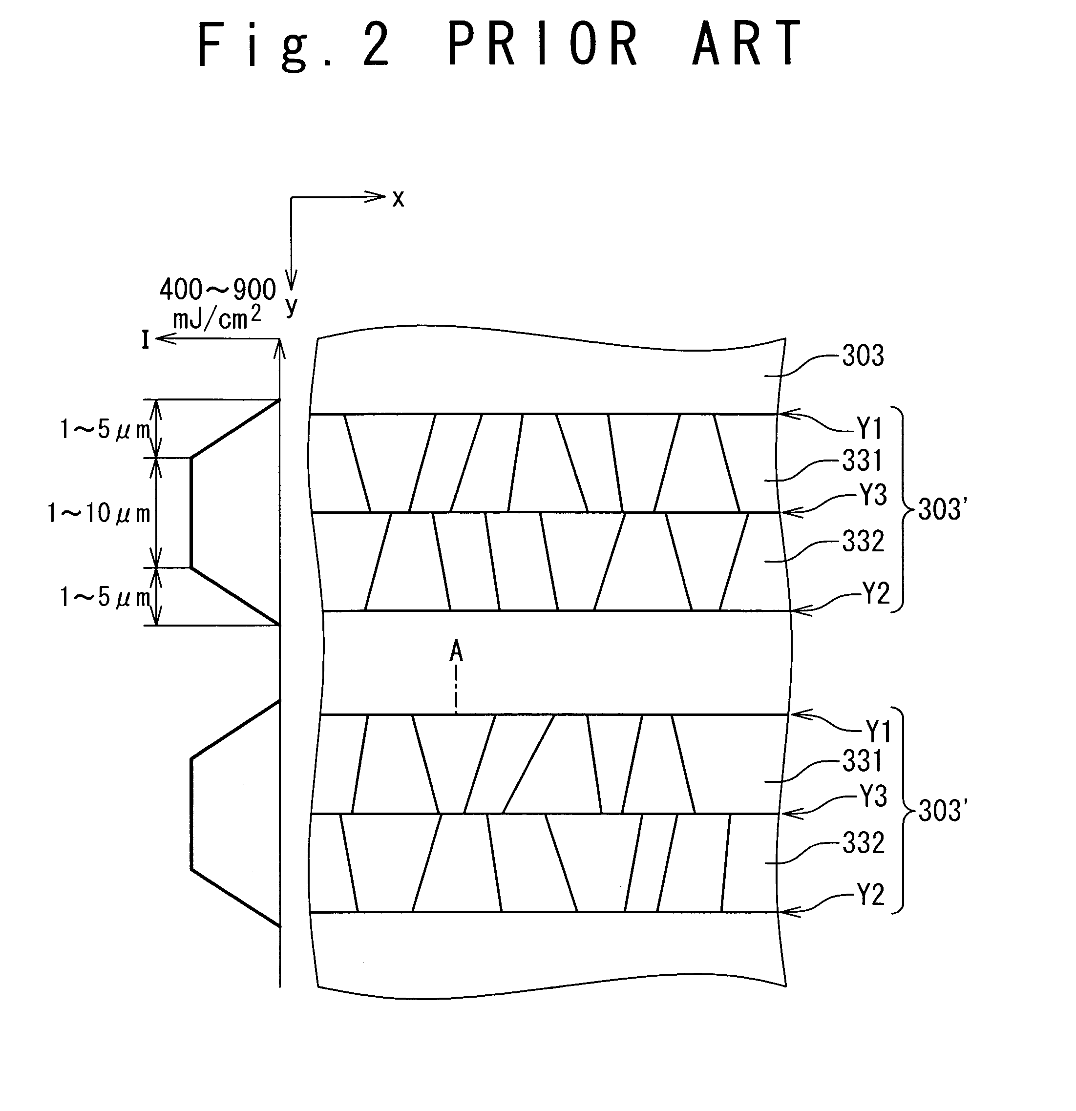
[0107]FIG. 17 shows results of the SEM observations of the crystallized films formed under the conditions with respective aperture intervals. The aperture intervals used are indicated at the bottom of respective images, and the scanning direction (first direction) is indicated by an arrow. As is clearly seen from FIG. 17, the appearances of the crystallized films vary with changing aperture intervals.

[0108] In the cases when the aperture interval is set to 0 μm or 0.6 μm, the influence of the shading section hardly appears in the SEM observation. In the case when the aperture interval is set to 0.9 μm, the difference in c...

Example

THIRD EXAMPLE

[0109] Another experiment is carried out as a third example, in which the shape of the beam shape is changed. The beam shape is rectangle as shown in FIG. 18. The beam width is a width of the beam cross section along the scanning direction (x direction in FIG. 18). The beam length is a length of the beam cross section along the second direction (y direction). The laser annealing apparatus similar to that in the first example is used to manufacture the semiconductor thin film. The experiment conditions according to the present example are shown in table 2. TABLE 2COMPARATIVEEXAMPLE 3EXAMPLELASER FLUENCE (mJ / cm2)480480STEP WIDTH (μm)0.20.2SCAN DISTANCE (μm)100100APERTURE WIDTH (μm)219.9APERTURE LENGTH (μm)12270


PUM


Abstract

A method of manufacturing a semiconductor thin film includes (A) forming an amorphous semiconductor film on a substrate, (B) irradiating a beam to a surface of the amorphous semiconductor film such that a predetermined region of the amorphous semiconductor film is melted and solidified to form a crystallized semiconductor film, and (C) scanning the beam in a first direction. A second direction is a direction on the surface of the amorphous semiconductor film perpendicular to the first direction. A length along the second direction of a cross section of the beam is substantially equal to or less than two times a width along the second direction of the crystallized semiconductor film.

Description

BACKGROUND OF THE INVENTION [0001] 1. Field of the Invention [0002] The present invention relates to a method of manufacturing a semiconductor thin film, an apparatus for manufacturing a semiconductor thin film, and a method of manufacturing a thin film transistor (TFT). More particularly, the present invention relates to a method of manufacturing a semiconductor thin film in which the formation of a grain boundary is controlled, and a thin film transistor having a layer of the semiconductor thin film. [0003] 2. Description of the Related Art [0004] As a display of an electronic product such as a personal computer and the like, a liquid crystal display (LCD) is known and widely used. In particular, an active matrix liquid crystal display (AM-LCD) has been rapidly popularized in recent years, because high quality images can be achieved due to switching devices provided for respective pixels. In the AM-LCD, a thin film transistor (referred to as “TFT”, hereinafter) is used as a switch...

Claims


Application Information

Patent Timeline
IPC IPC(8): C30B13/24H01L21/20H01L21/268H01L21/336H01L29/786
CPCC30B13/24H01L29/78675H01L29/66757H01L21/2026H01L21/02686H01L21/02488H01L21/02678H01L21/02422H01L21/02532H01L21/02691H01L21/0268
Inventor TAKAOKA, HIROMICHINAKATA, MITSURU
Owner VISTA PEAK VENTURES LLC
Why Eureka
Try Eureka