Semiconductor device having a gate insulating film structure including an insulating film containing metal, silicon and oxygen and manufacturing method thereof

Inactive Publication Date: 2005-01-13
HEAD TECHNOLOGY GMBH LTD +1
View PDF15 Cites 23 Cited by
  • Summary
  • Abstract
  • Description
  • Claims
  • Application Information

AI Technical Summary

Benefits of technology

[0012] Accordingly, the object of the present invention is to solve these problems by providing a semiconductor device having a metal oxide film or an insulating film containing metal, silicon and oxygen. Specifically, the present invention p

Problems solved by technology

However, when the metal oxide film is used as the gate insulating film, it is difficult to obtain a good interface which is free from distortion in a portion facing a silicon substrate.
Additionally, when the metal silicate film is used as the gate insulating film, a mediocre interface is attained, with a smaller dielectric constant than that of the metal oxide film.
Unfortunately, with time, the constituent metals of the two films become the same.
Therefore, it is difficult to attain the best

Method used


Image

  • Semiconductor device having a gate insulating film structure including an insulating film containing metal, silicon and oxygen and manufacturing method thereof
  • Semiconductor device having a gate insulating film structure including an insulating film containing metal, silicon and oxygen and manufacturing method thereof
  • Semiconductor device having a gate insulating film structure including an insulating film containing metal, silicon and oxygen and manufacturing method thereof

Examples


embodiment 1

[0041] Without wishing to unnecessarily limit the foregoing, the following shall discuss the invention with respect to certain preferred embodiments.

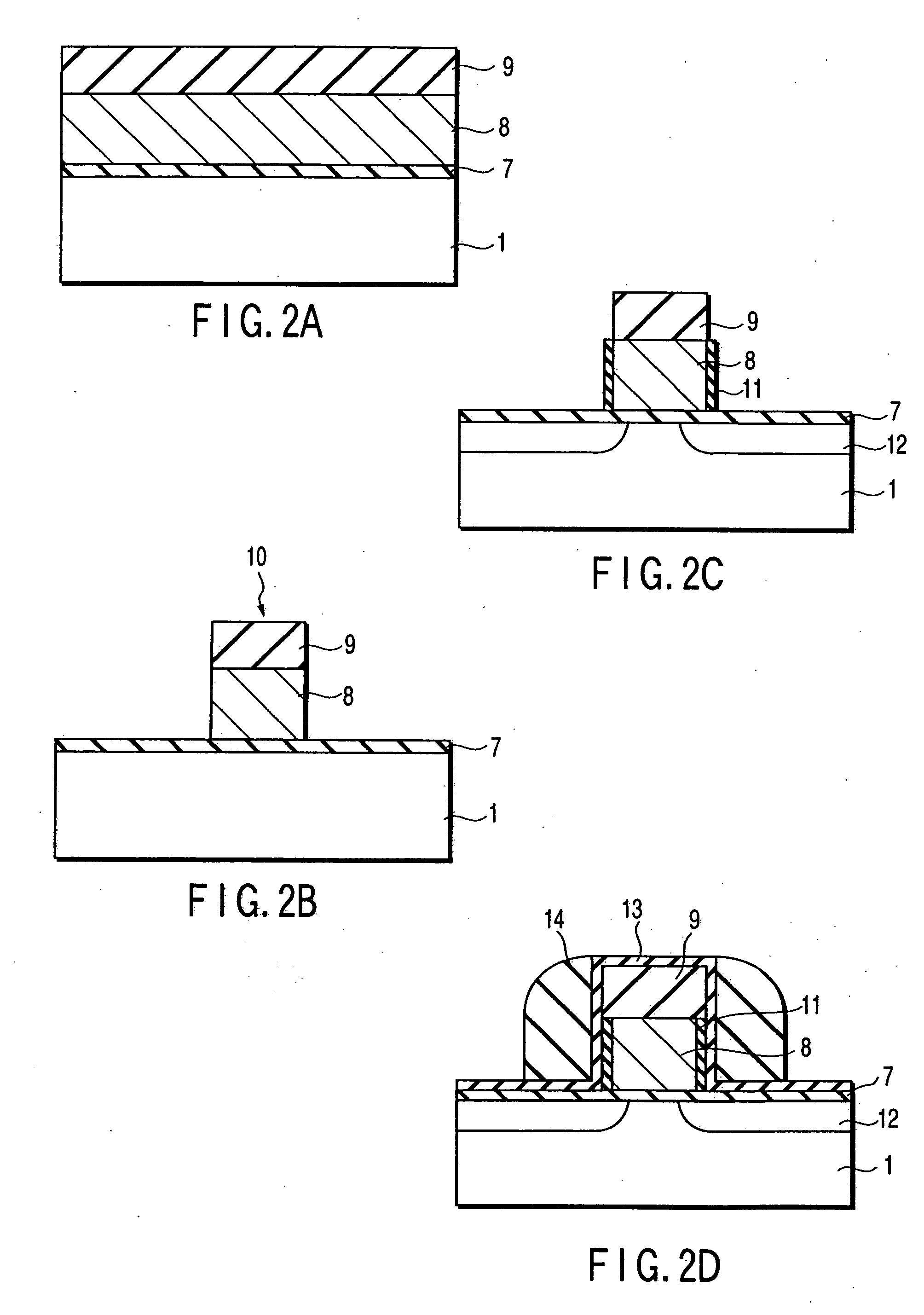
[0042] A first embodiment of this invention will now be described with reference to FIGS. 1A to 1B and 2A to 2I of the accompanying drawings.

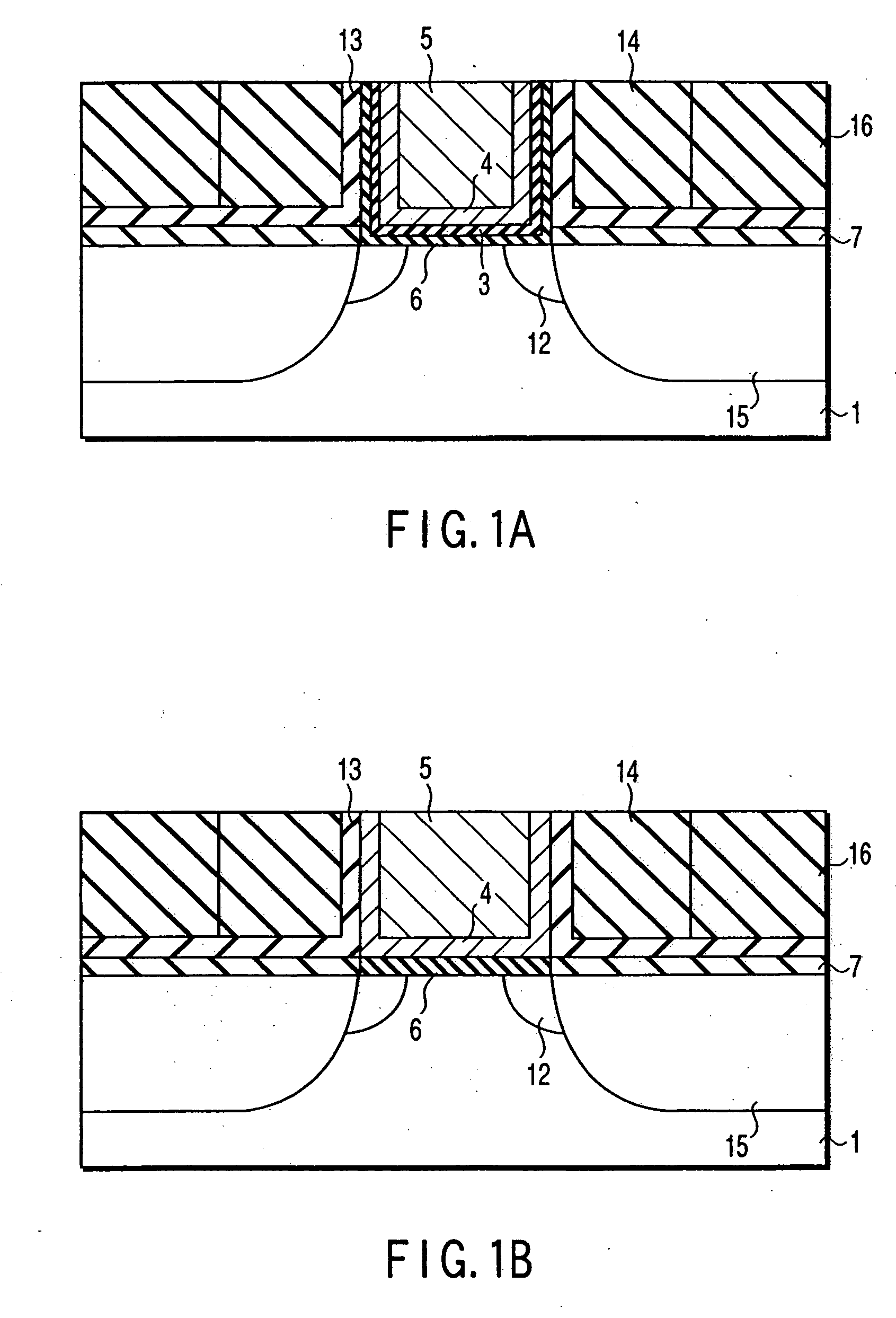
[0043]FIG. 1A shows a structure of a semiconductor device according to the first embodiment of this invention.

[0044] A metal silicon-oxygen material film (hereinafter a “metal silicate film”) 6 (which is a zirconium silicate film in accordance with this embodiment) as a compound of metal, silicon and oxygen, and a metal oxide film 3 (which is a zirconium oxide film in accordance with this embodiment) are formed as a gate insulating film on a silicon substrate 1. A titanium nitride film 4 is formed on metal oxide film 3 and a tungsten film 5 is formed on titanium nitride film 4 so as to fill a cavity formed on titanium nitride film 4 so that a multi-layered gate electrode is formed on metal oxide...

embodiment 2

[0069]FIG. 3 is a cross sectional view of a semiconductor device according to a second embodiment of this invention. The basic structure is similar to that of the embodiment 1 shown in FIG. 1A and portions of FIG. 3 which corresponds to those of FIG. 1A are denoted by the same reference numerals.

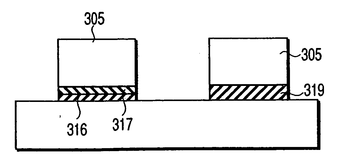
[0070] In the embodiment shown in FIG. 3, a zirconium silicate film 6 is formed only on the surface of a substrate 1, the film thickness thereof is approximately 1.5 nm, the film thickness of a zirconium oxide film 3 is approximately 3 nm, the film thickness obtained by converting the film thickness of each of these films into the film thickness of a silicon oxide film is approximately 0.5 nm and the total effective gate insulating film thickness is approximately 1 nm. In this embodiment, a small amount of nitrogen instead of fluorine is contained in zirconium silicate film 6 between the gate electrode and silicon substrate 1. The width of the gate electrode is approximately 50 nm.

[0071] I...

embodiment 3

[0090] The structure and manufacturing process of a semiconductor device according to an embodiment 3 of this invention will now be explained. The basic structure is similar to that of embodiment 2 shown in FIG. 3, except that the constituent material of the gate insulating film is amorphous. Embodiment 3 will now be explained with reference to FIG. 3.

[0091] Like embodiment 2, embodiment 3 uses zirconium oxide film as a metal oxide film 3 and a zirconium silicate film as a metal silicate film 6. The film thickness of zirconium silicate film 6 is approximately 1.5 nm, the film thickness of zirconium oxide film 3 is approximately 3 nm, the film thickness obtained by converting the film thickness of each of the above films 3 and 6 into the film thickness of a silicon oxide film is approximately 0.5 nm and the effective gate insulating film thickness is approximately 1 nm. The width of the gate electrode is approximately 50 nm.

[0092] Similar to embodiment 2, it is possible to use vari...


PUM

PropertyMeasurementUnit
Temperatureaaaaaaaaaa
Crystallization temperatureaaaaaaaaaa
aaaaaaaaaa

Abstract

Claimed and disclosed is a semiconductor device including a transistor having a gate insulating film structure containing nitrogen or fluorine in a compound, such as metal silicate, containing metal, silicon and oxygen, a gate insulating film structure having a laminated structure of an amorphous metal oxide film and metal silicate film, or a gate insulating film structure having a first gate insulating film including an oxide film of a first metal element and a second gate insulating film including a metal silicate film of a second metal element.

Description

RELATED APPLICATION [0001] This application claims priority to Japanese Application No. 2000-066960 filed Mar. 10, 2000, incorporated herein by reference. BACKGROUND OF THE INVENTION [0002] 1. Field of the Invention [0003] This invention is directed to a semiconductor device and a manufacturing method of the semiconductor device. More particularly to a semiconductor device having a gate insulating film structure including an insulating film which contains metal, silicon and oxygen, for example, a metal silicate film and the manufacturing method thereof. [0004] 2. Description of the Related Art [0005] It is desirable to make a thin gate insulating film for the miniaturization of the Metal Insulator Semiconductor Field Effect Transistor (“MISFET”). If a thin silicon oxide film or silicon oxide-nitride film is used as the gate insulating film, a leak current, that is, a direct tunnel current is increased due to a reduction in the film thickness. As a result, the minimum thickness is ap...

Claims


Application Information

Patent Timeline
IPC IPC(8): H01L21/28H01L21/316H01L21/336H01L21/8234H01L29/49H01L29/51H01L21/283H01L29/78
CPCH01L21/28088H01L29/6656H01L21/28194H01L21/28202H01L21/28211H01L21/31604H01L21/82345H01L21/823462H01L21/823475H01L29/4966H01L29/513H01L29/517H01L29/518H01L29/66545H01L21/28185H01L21/02271H01L21/02189H01L21/022H01L21/02159H01L21/18
Inventor TSUNASHIMA, YOSHITAKAIHUMIYA, SEIJISUIZU, YASUMASAOZAWA, YOSHIOMIYANO, KIYOTAKATANAKA, MASAYUKI
Owner HEAD TECHNOLOGY GMBH LTD
Why Eureka
Try Eureka